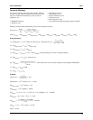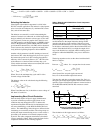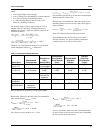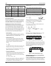
AN42 APPLICATION NOTE
2
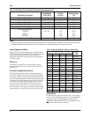
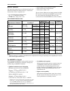
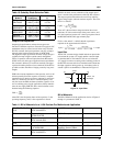
Table 2. Intel Pentium Pro and OverDrive Processor Power Specifications
Notes:
1. Maximum power values are measured at typical V
CC
P to take into account the thermal time constant of the CPU package.
2. Flexible motherboard specifications are recommendations only. Actual specifications are subject to change.
CPU Model & Features
Voltage
Specification
V
CC
P (VDC)
Maximum
Current
I
CC
P (A)
Maximum Thermal
Design Power
1
(W)
150MHz – 256K L2 Cache 3.1 ± 5% 9.9 29.2
166MHz – 512K L2 Cache 3.3 ± 5% 11.2 35.0
180MHz – 256K L2 Cache 3.3 ± 5% 10.1 31.7
200MHz – 256K L2 Cache 3.3 ± 5% 11.2 35.0
200MHz – 512K L2 Cache 3.3 ± 5% 12.4 37.9
OverDrive Processors
150 MHz 2.5 ± 5% 11.2 26.7
180 MHz 12.5 29.7
200 MHz 13.9 32.9
Flexible Motherboard
2
2.4-3.5 ± 5% 14.5 45.0
Output Ripple and Noise
Ripple and noise are defined as periodic or random signals
over the frequency band of 20MHz at the output pins. Output
ripple and noise requirements of ±1.0% must be met
throughout the full load range and under all specified input
voltage conditions.
Efficiency
The efficiency of the DC-DC converter must be greater
than 80% at high current draw and greater than 40% at low
current draw.
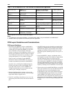
Processor Voltage Identification
The Pentium Pro package has four voltage identification
pins, VID3–VID0, that can be used for automatic selection
of the power supply voltage. These pins are internally uncon-
nected or are shorted to ground (V
SS
). The logic status of the
pins defines the voltage required by the processor. The VID
codes have been implemented to support voltage specifica-
tion variations on future Pentium Pro processors. These
codes are presented in Table 3. A ‘1’ refers to an open pin
and a ‘0’ refers to a short to ground. The V
CC
P power supply
should supply the voltage that is requested or disable itself.
Table 3. Voltage Identification Codes for Pentium Pro
I/O Controls
In addition to the voltage identification pins, several signals
exist to control the DC-DC converter or to provide feedback
from the converter to the CPU. These are Power-Good
(PWRGD), Output Enable (OUTEN), and Upgrade Present
(UP). These signals are discussed later.
Data Bits V
CC
P
VID3 VID2 VID1 VID0 (VDC)
1 1 1 1 No CPU
1 1 1 0 2.1
1 1 0 1 2.2
1 1 0 0 2.3
1 0 1 1 2.4
1 0 1 0 2.5
1 0 0 1 2.6
1 0 0 0 2.7
0 1 1 1 2.8
0 1 1 0 2.9
0 1 0 1 3.0
0 1 0 0 3.1
0 0 1 1 3.2
0 0 1 0 3.3
0 0 0 1 3.4
0 0 0 0 3.5


