AN42 APPLICATION NOTE
16
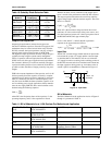
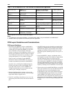
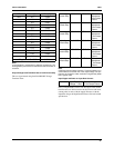
Refer to Appendix A for Directory of component suppliers.
Notes:
1. In synchronous mode using the RC5040, a 1A schottky diode (1N5817) may be substituted for the MBR1545CT.
2. MOSFET M3 is only required for the RC5040 synchronous application.
C13, C14, C15 Sanyo
6MV1500GX
1500µF 6.3V electrolytic
capacitor 10mm x 20mm
ESR < 0.047 Ω
DS1
(note 1)
Motorola
MBR1545CT
Shottky Diode Vf<0.72V @ If = 15A
DS2 General Instruments 1N5817 Schottky Diode 1A, 20V
L1 Skynet 320-8107 1.3µH inductor
L2* Skynet
320-6110
2.5µH inductor *Optional – will help re-
duce ripple on 5v line
M1, M2, M3
(note 2)
Fuji
2SK1388
N-Channel Logic Level
Enhancement Mode MOSFET
R
DS(ON)
< 37m ohm
V
GS
< 4V, I
D
> 20A
Rsense COPEL
A.W.G. #18
6 milliohm CuNi Alloy Wire
resistor
R1, R2, R3, R4, R6,
R7
Panasonic ERJ-6ENF10.0KV 10K 5% Resistors
U1 Raytheon
RC5042M or RC5040M
DC-DC Converter for Pentium
Pro
Table 11. Bill of Materials for a 14.5A Pentium Pro Motherboard Application
PCB Layout Guidelines and Considerations
PCB Layout Guidelines
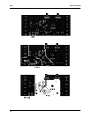
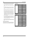
• Placement of the MOSFETs relative to the RC5040 is
critical. The MOSFETs (M1 & M2), should be placed
such that the trace length of the HIDRV pin to the FET
gate is minimized. A long lead length causes high
amounts of ringing due to the inductance of the trace and
the large gate capacitance of the FET. This noise radiates
all over the board, and because it is switching at a high
voltage and frequency, it is very difficult to suppress.
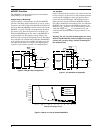
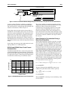
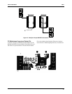
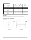
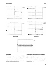
Figure 16 shows an example of proper MOSFET
placement in relation to the RC5040. It also shows an
example of problematic placement for the MOSFETs.
In general, noisy switching lines should be kept away
from the quiet analog section of the RC5040. That is,
traces that connect to pins 12 and 13 (HIDRV and
VCCQP) should be kept far away from the traces that
connect to pins 1 through 5, and pin 16.
• Place the 0.1µF decoupling capacitors as close to the
RC5040 and RC5042 pins as possible. Extra lead length
negates their ability to suppress noise.
• Each VCC and GND pin should have its own via to the
appropriate plane on the board to add isolation between
pins
• The CEXT timing capacitor should be surrounded with a
ground trace. The placement of a ground or power plane
underneath the capacitor provides further noise isolation,
and helps to shield the oscillator from the noise on the
PCB. This capacitor should be placed as close to pin 1 as
possible.
• Group the MOSFETs, inductor, and Schottky diode as
close together as possible. This minimizes ringing derived
from the inductance of the trace and the large gate
capacitance of the FET. Place the input bulk capacitors as
close to the drains of MOSFETs as possible. In addition,
place the 0.1µF decoupling capacitors right on the drain
of each MOSFET. This helps to suppress some of the high
frequency switching noise on the DC-DC converter input.
• The traces that run from the RC5040 IFB (pin 4) and VFB
(pin 5) pins should be run next to each other and be Kelvin
connected to the sense resistor. Running these lines
together helps to reject some of the common mode noise
to the RC5040 feedback input. Run the noisy switching
signals (HIDRV & VCCQP) on one layer, and use the
inner layers for power and ground only. If the top layer is
being used to route all of the noisy switching signals, use
the bottom layer to route the analog sensing signals VFB
and IFB.


