


5 - 10 C141-F037-02EN
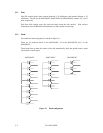
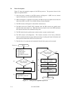
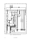
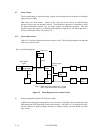
(2) Sample and hold circuit
The sample and hold circuit samples analog-waveform voltages according to the period of the
clock signals generated by the VFO circuit. The sample signal from the sample and hold circuit
is passed to the AGC gain controlling level detection circuit and VFO circuit.
(3) VFO circuit
The VFO circuit generates a clock signal that is synchronized with the sample and hold circuit
output signal. At data write, the VFO circuit generates a clock signal that is synchronized with
the clock signal from the synthesizer.
(4) Viterbi detection circuit
The viterbi detection circuit detects only the sample values above about 50% threshold level of
the sample and hold circuit output signal. Then this circuit decodes the nearest digital data to
actual data.
(5) 16/17 RLL decoding circuit
The 16/17 RLL decoding circuit decodes the viterbi detection circuit output signal. This
decoding circuit reverse converts (scrambles) the pseudorandom pattern (created at write) into
NRZ data. The NRZ data is then fed to the upper-level circuit.
(6) Sense current setup circuit
This disk drive uses MR heads, so the current applied to the heads is controlled by a digital-to-
analog converter. The sense current is set in units of heads.
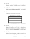
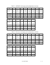
5.6.4 Write frequency change circuit
This disk drive uses the constant characteristics recording method for high density recording.
This recording method is different from the conventional recording method in which the write
frequency is fixed. With this new recording method, cylinders are grouped into several zones
depending on the drive type. The write frequency is changed so that the inner cylinder of each
zone has the same recording characteristics. The data area is split into 14 concentric circular
zones. Table 5.2 and 5.3 list the write frequency and recording density (bpi) of each zone.