D-3
Interface Information
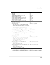
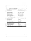
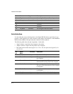
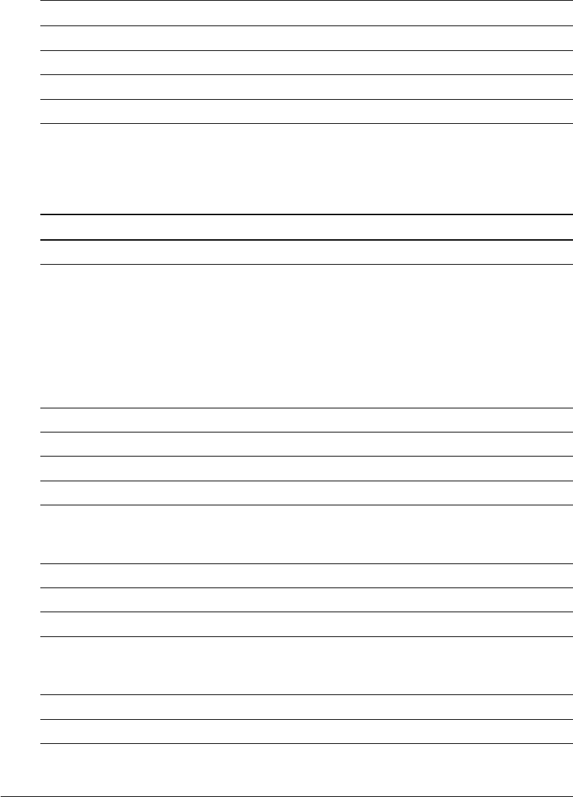
Pin Direction Signal Description
33 0 volts. Same as pins 14, 19-30.
34 Not used
35 Not used
36 Not used
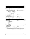
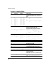
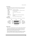
IEEE 1284-B Nibble Mode signals
The following table briefly gives connector pin assignments in IEEE 1284 mode.
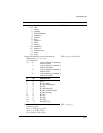
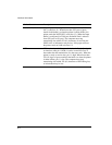
Pin Direction Signal Description
1 To printer HostClk High in reverse data transfer phase
2 To printer DATA BIT 1 These signals are the 1st to the 8th bits of
3 To printer DATA BIT 2 parallel data.
4 To printer DATA BIT 3
5 To printer DATA BIT 4 These signals are active high for a logical 1.
6 To printer DATA BIT 5
7 To printer DATA BIT 6
8 To printer DATA BIT 7
9 To printer DATA BIT 8
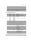
10 From printer PtrClk Set to low to qualify data on reverse channel
11 From printer PtrBusy Reverse channel: Data 3 and 7
12 From printer AckDataReq Reverse channel: Data 2 and 6
13 From printer Xflag Reverse channel: Data 1 and 5
14 To printer Host Busy Set to low to indicate that the host can
receive data
Set to high Host Acknowledge Receipt
15 Not used
16 0 volts. Logic ground
17 Chassis ground
18 From printer Peripheral Logic Set to high to indicate the printer is ON
High and all signals are in valid state.
- Max output current 50 mA
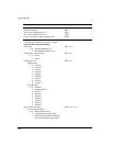
19-29 0 volts. Signal ground
30 0 volts. Signal ground


