


66 • Calibration
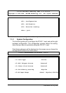
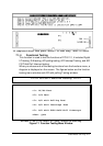
6.2 VR Assignment
There are five variable resistors (VR) on the PCI-9111 board to allow you
making accurate adjustment on A/D and D/A channels. The function of
each VR is specified as Table 6.1.
VR1 D/A full scale adjustment
VR2 D/A offset adjustment
VR3 A/D offset adjustment
VR4 A/D full scale adjustment
VR5 A/D programmable amplifier offset adjustment
Table 6.1 Functions of VRs
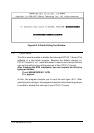
6.3 A/D Adjustment
1. Set the analog gain = 1 and channel number #0 by software.
2. Short the A/D channel 0 (pin 1 of CN3) to ground (GND), and
connect the TP1(+) and TP2(-) with your DVM. Trim the variable
resister VR5 to obtain a value as close as possible to 0V.
3. Applied a +10V reference input signal to A/D channel 0, and trim the
VR4 to obtain reading between 2046~2047(9111DG) or
32766~32767(9111HR).
4. Short the A/D channel 0 to ground, and trim the VR3 to obtain
reading flickers between 0~1.
5. Repeat step 3 and step 4, adjust VR4 and VR3.