Application Note
(Includes Differences for 970FX to 970MP)
IBM PowerPC
®
970MP RISC Microprocessor Preliminary
4. General Parameters
Page 10 of 25
AppNote_970FX-MP_Differences_Body.fm.1.0
November 15, 2006
4. General Parameters
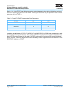
Table 4-1 provides a summary of the general parameters for the PowerPC 970FX and 970MP.
5. Design Enhancements for PowerPC 970MP
To create a dual core with improved power savings features, there were several enhancements made to the
PowerPC 970MP design.
This section describes the design enhancements to the 970MP.
5.1 Dual Core Design
The 970MP chip consists of two processing units (PUs), each containing an execution core with L1 caches, a
storage subsystem including L2 cache, and pervasive functions. In addition, a small amount of common logic
that is outside either PU is included to interface each PU to the single bus interface.
The two cores function as would two cores on separate chips for the most part. For example, they maintain
memory coherence via the bridge chip, they are able to Doze independently, and they have private access to
most processor resources including the L2. Also, like processors on separate chips, they scale frequency,
using the power tuning facility, together.
Sharing the same chip constrains the behavior of the two cores in several ways. First, the two PUs have
separate voltage planes for power, but the core voltages will always need to be within the delta specified in
the IBM PowerPC 970MP RISC Microprocessor Datasheet when the two processors are running. Also, the
core frequencies will always be the same. This would be true for two separate cores except for the Deep Nap
case, where one of two separate processors could reduce frequency to 1/64, while the other ran at functional
speed. The two 970MP cores must go into and come out of Deep Nap together.
The other difference between having dual cores on a single chip, versus two separate chips, is that they
share a single PI (processor interconnect) interface to the bridge chip. This requires that the interface
between the BIU and the PI logic be enhanced with buffers and muxes to support the sharing of the PI inter-
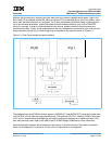
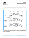
face between the two cores. Figure 5-1 on page 11 shows the relationship among the two cores and the
common logic.
For incoming PI data and commands, the output of the PI decoder is passed directly to both processors. For
outgoing PI data and commands, an arbiter and mux are introduced in front of the PI encoder to give one or
the other processor access to the outgoing PI bus at any given time. The arbiter implements a round robin
Table 4-1. General Parameters of the PowerPC 970FX and 970MP
Item 970FX Description 970MP Description
Die Size 66.2 sq. mm 153.8 sq. mm
Die Dimensions 7.07mm x 9.36mm 13.225 mm x 11.629 mm
Transistor Count 52 million 183 Million
Logic Design Static with some dynamic logic Static with some dynamic logic
Package
576-pin Ceramic ball grid array (CBGA)
25x25mm (1.0mm pitch)
575-pin Ceramic ball grid array (CBGA)
25x25mm (1.0mm pitch)


