


Application Note
(Includes Differences for 970FX to 970MP)
Preliminary IBM PowerPC
®
970MP RISC Microprocessor
AppNote_970FX-MP_Differences_Body.fm.1.0
November 15, 2006
5. Design Enhancements for PowerPC 970MP
Page 13 of 25
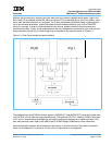
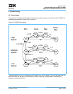
5.2 Processor Interconnect Bus
The 970MP design incorporates an enhanced Processor Interconnect (PI) Interface for its high-speed off-chip
bus. There are a number of changes to the physical interface and support hardware associated with the use
of the enhanced definition from that in the 970FX. These changes include modifications to the driver and
receiver, two new test modes of operation, and additional control and status registers.
5.2.1 SCOM control and status registers
The 970FX contains five 32-bit SCOM registers associated with PI (x’04.6A00’, x’0F.6A01’, x’0F.7A00’,
x’04.6B01’, x’0F.6B00’, and x’0F.7B01’). Three of these are mode registers and two are status registers. See
the IBM PowerPC 970FX RISC Microprocessor User’s Manual for a description of these registers. The
970MP replaces these five SCOM registers with a set of sixteen new SCOM registers (located in the common
domain at address x’08.XXXX’). Eight of these are 16-bit registers for fault isolation and error reporting. One
is a 16-bit command register for specifying a clock delay. Two are 64-bit IAP registers that allow programming
of the IAP pattern. Four are 16-bit mode registers. One is a 16-bit status register. This status register is a
read-only register that can be programmed by bits in a mode register (mode register 2, bit 48:54) to return the
status of different aspects of the PI interface, depending on the mode register values. These registers are
only accessible by the master processing unit. The IBM PowerPC 970MP Microprocessor User’s Manual
describes these registers in detail.
Note in particular the different use of the windage field in the 970MP compared with that in the 970FX. In the
970MP, the windage field is used to add a fixed amount of delay to all bits prior to IAP learning, in order to
avoid an underflow when a guardbanding procedure is performed at the end of the IAP.
5.2.2 Test Modes
Two new test modes are supported for bringup of the PI interface. These are the electrical shorts test (EST)
and the pseudo-random data test (RDT). The following sections describe both the transmitter and receiver
support for these functions.
5.2.2.1 Transmitter Pseudo-Random Data Test (RDT)
One new test feature is the pseudo-random data test mode. This mode uses a built in linear feedback shift
register (LFSR) to create pseudo-random patterns to be transmitted across each enabled channel. The LFSR
register is 12 bits wide and implements the polynomial 1+x
3
+x
5
+x
11
, using a seed of all 1 bits. These data
patterns can then be received and compared to expected patterns created in the receiver core. This mode is
described in more detail in the corresponding receiver section. Pseudo-random test mode is enabled by
setting the following combination of I/O SCOM mode register 0 bits: WIAP to ‘1’, RDTMODE to ‘1’ and
ESTMODE to ‘0’. The pseudo-random patterns are created as long as this bit combination is set.
5.2.2.2 Transmitter Electrical Shorts Test (EST)
The second new test feature supports a mode which allows the integrity of the off-chip link to be tested to
verify its electrical integrity - that is, to find opens and shorts between channels. In support of this feature, the
transmitter core can create specific patterns that are then verified in the receiver core. Described below are
the patterns created by the transmitter for this mode. This mode is described in detail in the corresponding
receiver section. In short test mode, the transmitter creates a pattern of 16 consecutive data ‘1’ bits on serial
data channel 0, while all other channels are transmitting ‘0’ bits. After 16 bit times, the next sequential
channel will transmit a data ‘1’ for 16 bit times, while the previously enabled channel and all other channels