


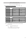


121
CHAPTER 10 A/D CONVERTER
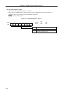
(1) Successive approximation register (SAR)
This register compares the analog input voltage value to the voltage tap (compare voltage) value applied from
the series resistor string and holds the result from the most significant bit (MSB).
When held to the least significant bit (LSB) (end of A/D conversion), the contents of the SAR are transferred
to the A/D conversion results register.
(2) A/D conversion result register (ADCR)
This register holds the A/D conversion result. Each time A/D conversion terminates, the conversion result
is loaded from the successive approximation register.
ADCR is read with an 8-bit memory manipulation instruction.
RESET input makes ADCR undefined.
(3) Sample & hold circuit
The sample & hold circuit samples each analog input signal sequentially applied from the input circuit and
sends it to the voltage comparator. This circuit holds the sampled analog input voltage value during A/D
conversion.
(4) Voltage comparator
The voltage comparator compares the analog input to the series resistor string output voltage.
(5) Series resistor string
The series resistor string is connected within AV
REF to AVSS and generates a voltage for comparison with the
analog input.
(6) ANI0 to ANI7 pins
These are 8-channel analog input pins to input analog signals to undergo A/D conversion to the A/D converter.
Pins other than those selected as analog input by the A/D converter input select register (ADIS) can be used
as input/output ports.
Caution Use ANI0 to ANI7 input voltages within the specified range. If a voltage higher than AV
REF
or lower than AVSS is applied (even if within the absolute maximum ratings), the converted
value of the corresponding channel becomes indeterminate and may adversely affect the
converted values of other channels.
(7) AV
REF pin
This pin inputs the A/D converter reference voltage.
It converts signals input to ANI0 to ANI7 into digital signals according to the voltage applied between AV
REF
and AVSS.
The current flowing in the series resistor string can be reduced by setting the voltage to be input to the AV
REF
pin to AVSS level in standby mode.
(8) AV
SS pin
This is a GND potential pin of the A/D converter. Keep it at the same potential as the V
SS pin when not using
the A/D converter.
(9) AV
DD pin
This is an A/D converter analog power supply pin. Keep it at the same potential as the V
SS pin when not using
the A/D converter.