


29
CHAPTER 3 CPU ARCHITECTURE
3.1.2 Internal data memory space
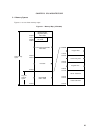
The internal high speed RAM configuration is 256 × 8-bit in the
µ
PD78081, 384 × 8-bit in the
µ
PD78082 and 512
× 8-bit in the
µ
PD8P083. In this area, four banks of general registers, each bank consisting of eight 8-bit registers,
are allocated in the 32-byte area FEE0H to FEFFH.
The internal high-speed RAM can also be used as a stack memory area.
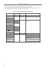
3.1.3 Special Function Register (SFR) area
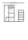
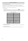
An on-chip peripheral hardware special-function register (SFR) is allocated in the area FF00H to FFFFH. (Refer
to Table 3-2. Special-Function Register List in 3.2.3 Special Function Register (SFR)).
Caution Do not access addresses where the SFR is not assigned.
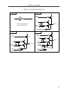
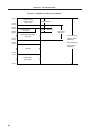
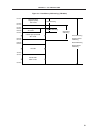
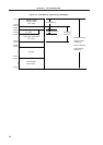
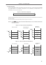
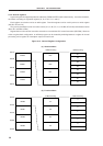
3.1.4 Data memory addressing
The method to specify the address of the instruction to be executed next, or the address of a register or memory
to be manipulated when an instruction is executed is called addressing.
The address of the instruction to be executed next is addressed by the program counter PC (for details, refer to
3.3 Instruction Address Addressing).
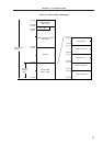
To address the memory that is manipulated when an instruction is executed, the
µ
PD78083 Subseries is provided
with many addressing modes with a high operability. Especially at addresses corresponding to data memory area,
particular addressing modes are possible to meet the functions of the special function registers (SFRs) and general
registers. This area is between FE00H and FFFFH for the
µ
PD78081, FD80H and FFFFH for the
µ
PD78082, and
between FD00H and FFFFH for the
µ
PD78P083. The data memory space is the entire 64K-byte space (0000H to
FFFFH). Figure 3-4 to 3-6 show the data memory addressing modes. For details of each addressing, refer to 3.4
Operand Address Addressing.