


8086
EXTERNAL SYNCHRONIZATION VIA TEST
As an alternative to the interrupts and general IO
capabilities the 8086 provides a single software-
testable input known as the TEST
signal At any time
the program may execute a WAIT instruction If at
that time the TEST
signal is inactive (HIGH) pro-
gram execution becomes suspended while the proc-
essor waits for TEST
to become active It must
remain active for at least 5 CLK cycles The WAIT
instruction is re-executed repeatedly until that time
This activity does not consume bus cycles The
processor remains in an idle state while waiting All
8086 drivers go to 3-state OFF if bus ‘‘Hold’’ is en-
tered If interrupts are enabled they may occur while
the processor is waiting When this occurs the proc-
essor fetches the WAIT instruction one extra time
processes the interrupt and then re-fetches and re-
executes the WAIT instruction upon returning from
the interrupt
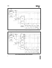
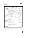
Basic System Timing
Typical system configurations for the processor op-
erating in minimum mode and in maximum mode are
shown in Figures 4a and 4b respectively In mini-
mum mode the MNMX
pin is strapped to V
CC
and
the processor emits bus control signals in a manner
similar to the 8085 In maximum mode the MNMX
pin is strapped to V
SS
and the processor emits cod-
ed status information which the 8288 bus controller
uses to generate MULTIBUS compatible bus control
signals Figure 5 illustrates the signal timing relation-
ships
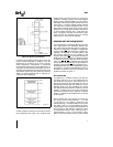
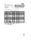
231455–10
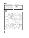
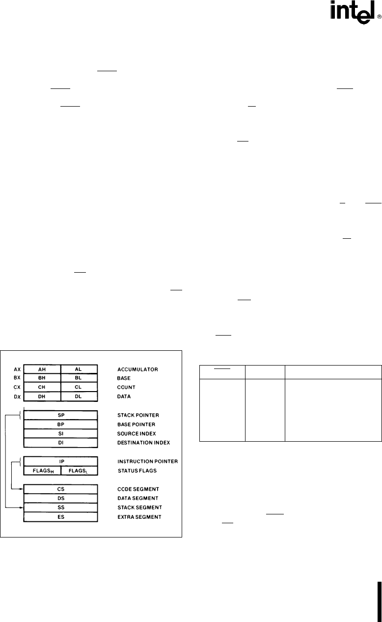
Figure 7 8086 Register Model
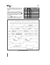
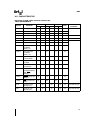
SYSTEM TIMINGMINIMUM SYSTEM
The read cycle begins in T
1
with the assertion of the
Address Latch Enable (ALE) signal The trailing (low-
going) edge of this signal is used to latch the ad-
dress information which is valid on the local bus at
this time into the address latch The BHE
and A
0
signals address the low high or both bytes From T
1
to T
4
the MIO signal indicates a memory or IO
operation At T
2
the address is removed from the
local bus and the bus goes to a high impedance
state The read control signal is also asserted at T
2
The read (RD
) signal causes the addressed device
to enable its data bus drivers to the local bus Some
time later valid data will be available on the bus and
the addressed device will drive the READY line
HIGH When the processor returns the read signal to
a HIGH level the addressed device will again 3-
state its bus drivers If a transceiver is required to
buffer the 8086 local bus signals DTR
and DEN
are provided by the 8086
A write cycle also begins with the assertion of ALE
and the emission of the address The MIO
signal is
again asserted to indicate a memory or IO write
operation In the T
2
immediately following the ad-
dress emission the processor emits the data to be
written into the addressed location This data re-
mains valid until the middle of T
4
During T
2
T
3
and
T
W
the processor asserts the write control signal
The write (WR
) signal becomes active at the begin-
ning of T
2
as opposed to the read which is delayed
somewhat into T
2
to provide time for the bus to float
The BHE
and A
0
signals are used to select the prop-
er byte(s) of the memoryIO word to be read or writ-
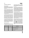
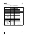
ten according to the following table
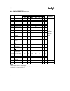
BHE A0 Characteristics
0 0 Whole word
0 1 Upper byte fromto
odd address
1 0 Lower byte fromto
even address
1 1 None
IO ports are addressed in the same manner as
memory location Even addressed bytes are trans-
ferred on the D
7
–D
0
bus lines and odd addressed
bytes on D
15
–D
8
The basic difference between the interrupt acknowl-
edge cycle and a read cycle is that the interrupt ac-
knowledge signal (INTA) is asserted in place of the
read (RD
) signal and the address bus is floated
(See Figure 6) In the second of two successive
INTA cycles a byte of information is read from bus
12