


8086
231455–3
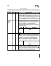
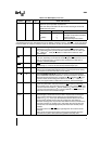
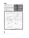
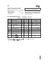
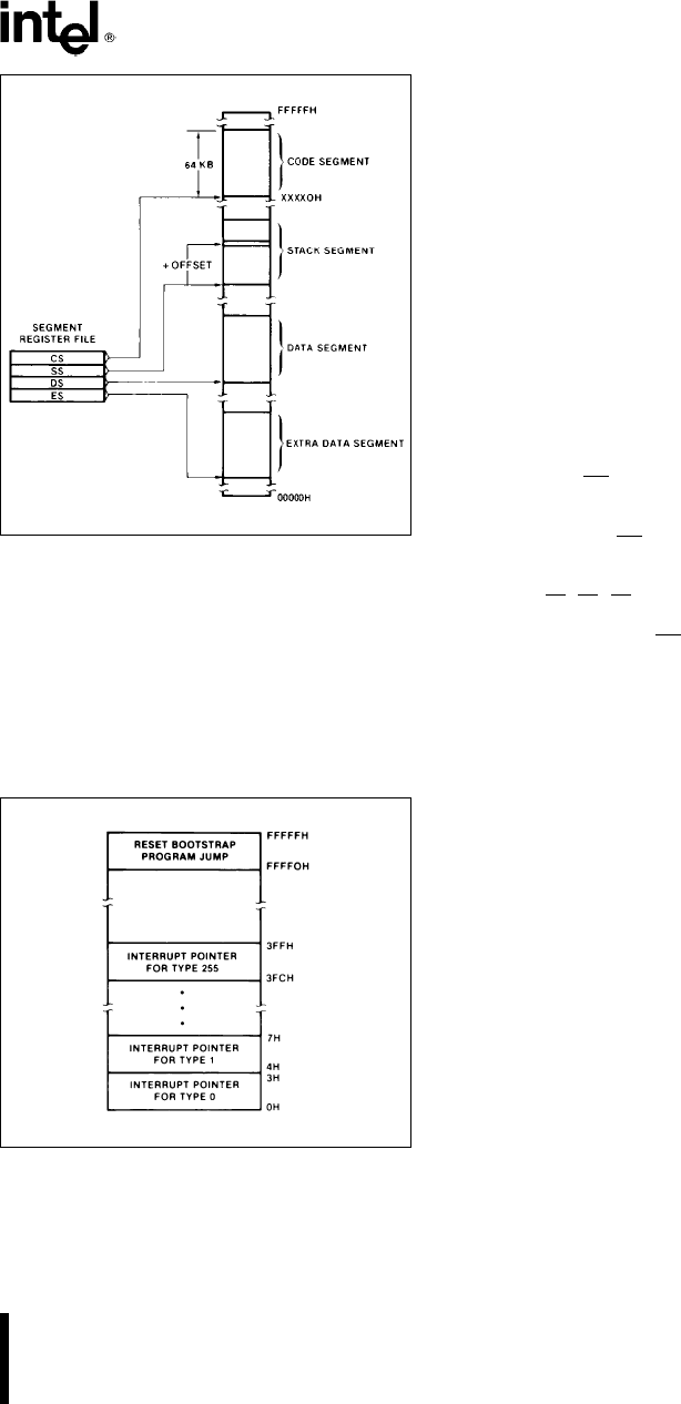
Figure 3a Memory Organization
In referencing word data the BIU requires one or two
memory cycles depending on whether or not the
starting byte of the word is on an even or odd ad-
dress respectively Consequently in referencing
word operands performance can be optimized by lo-
cating data on even address boundaries This is an
especially useful technique for using the stack since
odd address references to the stack may adversely
affect the context switching time for interrupt pro-
cessing or task multiplexing
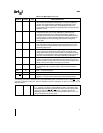
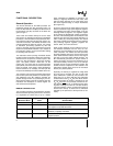
231455–4
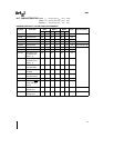
Figure 3b Reserved Memory Locations
Certain locations in memory are reserved for specific
CPU operations (see Figure 3b) Locations from
address FFFF0H through FFFFFH are reserved for
operations including a jump to the initial program
loading routine Following RESET the CPU will al-
ways begin execution at location FFFF0H where the
jump must be Locations 00000H through 003FFH
are reserved for interrupt operations Each of the
256 possible interrupt types has its service routine
pointed to by a 4-byte pointer element consisting of
a 16-bit segment address and a 16-bit offset ad-
dress The pointer elements are assumed to have
been stored at the respective places in reserved
memory prior to occurrence of interrupts
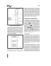
MINIMUM AND MAXIMUM MODES
The requirements for supporting minimum and maxi-
mum 8086 systems are sufficiently different that
they cannot be done efficiently with 40 uniquely de-
fined pins Consequently the 8086 is equipped with
a strap pin (MNMX
) which defines the system con-
figuration The definition of a certain subset of the
pins changes dependent on the condition of the
strap pin When MNMX
pin is strapped to GND the
8086 treats pins 24 through 31 in maximum mode
An 8288 bus controller interprets status information
coded into S
0
S
2
S
2
to generate bus timing and
control signals compatible with the MULTIBUS ar-
chitecture When the MNMX
pin is strapped to V
CC
the 8086 generates bus control signals itself on pins
24 through 31 as shown in parentheses in Figure 2
Examples of minimum mode and maximum mode
systems are shown in Figure 4
BUS OPERATION
The 8086 has a combined address and data bus
commonly referred to as a time multiplexed bus
This technique provides the most efficient use of
pins on the processor while permitting the use of a
standard 40-lead package This ‘‘local bus’’ can be
buffered directly and used throughout the system
with address latching provided on memory and IO
modules In addition the bus can also be demulti-
plexed at the processor with a single set of address
latches if a standard non-multiplexed bus is desired
for the system
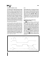
Each processor bus cycle consists of at least four
CLK cycles These are referred to as T
1
T
2
T
3
and
T
4
(see Figure 5) The address is emitted from the
processor during T
1
and data transfer occurs on the
bus during T
3
and T
4
T
2
is used primarily for chang-
ing the direction of the bus during read operations In
the event that a ‘‘NOT READY’’ indication is given
by the addressed device ‘‘Wait’’ states (T
W
) are in-
serted between T
3
and T
4
Each inserted ‘‘Wait’’
state is of the same duration as a CLK cycle Periods
7