


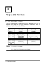
Registers Format
•
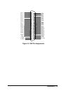
17
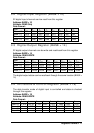
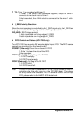
3.2 Digital Input Register (BASE + 10)
32 digital input channels can be read from this register
Address: BASE + 10
Attribute: READ Only
Data Format:
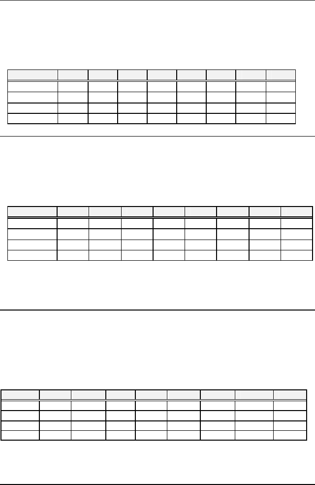
Byte 7 6 5 4 3 2 1 0
Base +10 DI7 DI6 DI5 DI4 DI3 DI2 DI1 DI0
Base +11 DI15 DI14 DI13 DI12 DI11 DI10 DI9 DI8
Base +12 DI23 DI22 DI21 DI20 DI19 DI18 DI17 DI16
Base +13 DI31 DI30 DI29 DI28 DI27 DI26 DI25 DI24
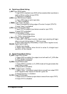
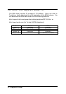
3.3 Digital Output Register (BASE + 14)
32 digital output channels can be write and read-back from this register
Address: BASE + 14
Attribute: READ/WRITE
Data Format:
Byte 7 6 5 4 3 2 1 0
Base +14 DO7 DO6 DO5 DO4 DO3 DO2 DO1 DO0
Base +15 DO15 DO14 DO13 DO12 DO11 DO10 DO9 DO8
Base +16 DO23 DO22 DO21 DO20 DO19 DO18 DO17 DO16
Base +17 DO31 DO30 DO29 DO28 DO27 DO26 DO25 DO24
The digital output status can be read back through the same location (BASE +
14)
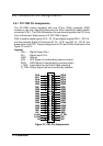
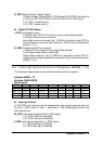
3.4 DIO Status & Control Register (BASE + 18)
The data transfer mode of digital input is controlled and status is checked
through this register.
Address: BASE + 18
Attribute: READ/WRITE
Data Format:
Byte 7 6 5 4 3 2 1 0
Base +18 O_ACK DIN_EN I_TRG TRGPL I_FIFO I_TIME0 I_REQ I_ACK
Base +19 ---- I_OVER ---- ---- O_TRG O_FIFO O_TIME1 O_REQ
Base +20 ---- ---- ---- ---- ---- ---- ---- O_UND
Base +21 ---- ---- ---- ---- ---- ---- ---- ----