


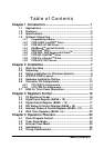


Table of Contents
•
i
Table of Contents
Chapter 1 Introduction............................................................. 1
1.1 Applications....................................................................1
1.2 Features..........................................................................2
1.3 Specifications.................................................................2
1.4 Software Supporting.......................................................4
1.4.1 Programming Library..................................................................4
1.4.2 PCIS-LVIEW: LabVIEW
®
Driver.................................................5
1.4.3 PCIS-VEE: HP-VEE Driver..........................................................5
1.4.4 DAQBench
TM
: ActiveX Controls ...............................................5
1.4.5 DASYLab
TM
PRO...........................................................................5
1.4.6 PCIS-DDE: DDE Server and InTouch
TM
.................................5
1.4.7 PCIS-ISG: ISaGRAF
TM
driver .....................................................6
1.4.8 PCIS-ICL: InControl
TM
Driver.....................................................6
1.4.9 PCIS-OPC: OPC Server...............................................................6
Chapter 2 Installation............................................................... 7
2.1 What You Have ...............................................................7
2.2 Unpacking.......................................................................8
2.3 Device Installation for Windows Systems.......................8
2.4 cPCI/PCI-7200’s Layout...................................................9
2.5 Hardware Installation Outline .......................................11
2.6 Connector Pin Assignments.........................................12
2.6.1 PCI-7200 Pin Assignments......................................................12
2.6.2 cPCI-7200 Pin Assignments....................................................14
2.7 8254 for Timer Pacer Generation..................................15
Chapter 3 Registers Format .................................................16
3.1 I/O Registers Format.....................................................16
3.2 Digital Input Register (BASE + 10)................................17
3.3 Digital Output Register (BASE + 14) .............................17
3.4 DIO Status & Control Register (BASE + 18) ..................17
3.5 Interrupt Status & Control Register (BASE + 1C)..........19
3.6 8254 Timer Registers (BASE + 0) ..................................22
Chapter 4 Operation Theorem.............................................23
4.1 Direct Program Control.................................................23
4.2 Timer Pacer Mode.........................................................24
4.3 External Clock Mode.....................................................25
4.4 Handshaking.................................................................25
4.5 Timing Characteristic....................................................27