


20
•
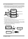
Registers Format
T0_EN: Interrupt is triggered by timer 0 output.
1: Timer 0 interrupt is enabled
0: Timer 0 interrupt is disabled
T1_EN: Interrupt is triggered by timer 1 output.
1: Timer 1 interrupt is enabled
0: Timer 1 interrupt is disabled
T2_EN: Interrupt is triggered by timer 2 output.
1: Timer 2 interrupt is enabled
0: Timer 2 interrupt is disabled
u Interrupt Status:
The following bits are used to check interrupt status:
SO_ACK: Status of O_ACK interrupt
1: O_ACK Interrupt occurred
0: No O_ACK interrupt
SI_REQ: Status of I_REQ interrupt
1: I_REQ Interrupt occurred
0: No I_REQ Interrupt
SI_T0: Status of timer 0 interrupt
1: OUT0 (output of timer 0) Interrupt occurred
0: No timer 0 Interrupt
SI_T1: Status of timer 1 interrupt
1: OUT1 (output of timer 1) Interrupt occurred
0: No timer 1 Interrupt
SI_T2: Status of timer 2 interrupt
1: OUT2 (output of timer 2) interrupt occurred
0: No timer 2 Interrupt
Note: Writing 1 to the corresponding bit of the register can clear all the
interrupt status. In order to make the interrupt work properly, the
interrupt service routine has to clear all the interrupt status before end
of the ISR.
u Timer Configuration Control:
The 8254 timer on the PCI-7200 can be configured as either timer 0 cascaded
with timer 2 or timer 1 cascaded w ith timer2. These configuration are controlled
by the following bits:
T0_T2: Timer 0 is cascaded with timer 2
1: Timer 0 and timer 2 are cascaded together, output of timer 2
connects to the clock input of timer 0.
0: Not cascaded, the 4 MHz clock is connected to the timer 0 clock
input.