


Operation Theorem
•
25
4.3 External Clock Mode
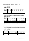
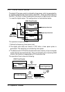
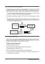
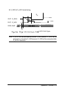
The digital input is clocked by external strobe, which is from the Pin 19 (I_REQ)
of CN2 (PCI-7200) or Pin 24 of CN1 (cPCI-7200). The operation sequence is
very similar to Timer Pacer Trigger. The only difference is the clock source.
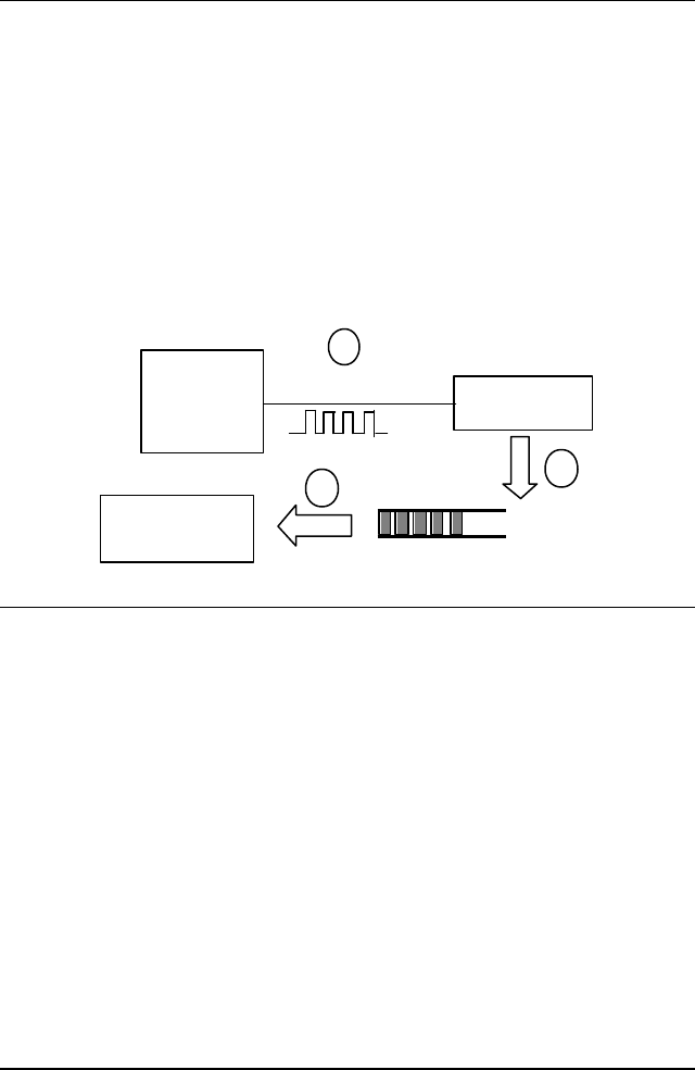
1. The external input strobe is generated from outside device, and go through
the Pin 19 (I_REQ) of CN2 and to latch the digital input.
2. The digital input data are saved in FIFO after an I/O strobe signal is coming
in.
3. The data saved in input FIFO will be transferred to main memory on your
computer system directly. This is controlled by bus mastering DMA control,
this function is supported by PCI
To Digital Input Trigger
Latch Digital
Input Data
Digital Input FIFO
Bus mastering
DMA data Transfer
PC's Main Memory
1
2
3
Pin 19 of CN2
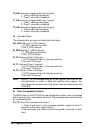
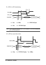
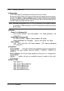
4.4 Handshaking
In PCI-7200, it also supports a handshaking digital I/O transfer mode. That is,
after input data is ready, an I_REQ is sent form external device, and I_ACK will
go high to acknowledge the data already accessed.
I_REQ & I_ACK for Digital Input
1. Digital Input Data is ready
2. An I_REQ signal is generated for digital input operation
3. Digital input data is saved to FIFO
4. An I_ACK signal is generated and sent to outside device
5. If the FIFO is not empty and PCI bus is not occupied, the data will be
transferred to main memory