


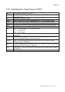
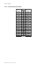
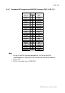

ECB-870
ECB-870 User’s Manual 31
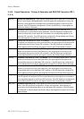
PDIOR# Primary Disk IO Read. In normal IDE this is the command to the IDE device that it may drive
data onto the PDD [15:0] lines. Data is latched by PIIX4 on the negation edge of PDIOR#. The
IDE device is selected either by the ATA register file chip selects (PDCS1#, PDCS3#) and the
PDA [2:0] lines, or the IDE DMA slave arbitration signals (PDDACK#).
In an Ultra DMA/33 read cycle, this signal is used as DMARDY# which is negated by the PIIX4
to pause Ultra DMA/33 transfers. In an Ultra DMA/33 write cycle, this signal is used as the
STROBE signal, with the drive latching data on rising and falling edges of STROBE.
If the IDE signals are configured for Primary and Secondary, this signal is connected to the
corresponding signal on the Primary IDE connector. If the IDE signals are configured for
Primary Master and Primary Slave, this signal is used for the Primary Master connector.
SDIOR# Secondary Disk IO Read. In normal IDE mode, this is the command to the IDE device that it
may drive data onto the SDD [15:0] lines. Data is latched by the PIIX4 on the negation edge of
SDIOR#. The IDE device is selected either by the ATA register file chip selects (SDCS1#,
SDCS3#) and the SDA [2:0] lines, or the IDE DMA slave arbitration signals (SDDACK#).
In an Ultra DMA/33 read cycle, this signal is used as DMARDY# which is negated by the PIIX4
to pause Ultra DMA/33 transfers. In an Ultra DMA/33 write cycle, this signal is used as the
STROBE signal, with the drive latching data on rising and falling edges of STROBE.
If the IDE signals are configured for Primary and Secondary, this signal is connected to the
corresponding signal on the Secondary IDE connector. If the IDE signals are configured for
Primary Master and Primary Slave, these signals are used for the Primary Slave connector.
PDIOW# Primary Disk IO Write. In normal IDE mode, this is the command to the IDE device that it
may latch data from the PDD [15:0] lines. Data is latched by the IDE device on the negation
edge of PDIOW#. The IDE device is selected either by the ATA register file chip selects
(PDCS1#, PDCS3#) and the PDA [2:0] lines, or the IDE DMA slave arbitration signals
(PDDACK#).
For Ultra DMA/33 mode, this signal is used as the STOP signal, which is used to terminate an
Ultra DMA/33 transaction. If the IDE signals are configured for Primary and Secondary, this
signal is connected to the corresponding signal on the Primary IDE connector.
If the IDE signals are configured for Primary Master and Primary Slave, this signal is used for
the Primary Master connector.
SDIOW# Secondary Disk IO Write. In normal IDE mode, this is the command to the IDE device that it
may latch data from the SDD [15:0] lines. Data is latched by the IDE device on the negation
edge of SDIOW#. The IDE device is selected either by the ATA register file chip selects
(SDCS1#, SDCS3#) and the SDA [2:0] lines, or the IDE DMA slave arbitration signals
(SDDACK#).
In read and write cycles this signal is used as the STOP signal, which is used to terminate an
Ultra DMA/33 transaction.
If the IDE signals are configured for Primary and Secondary, this signal is connected to the
corresponding signal on the Secondary IDE connector.
If the IDE signals are configured for Primary Master and Primary Slave, these signals are used
for the Primary Slave connector.