


Board Manual 71
Software Reference 5
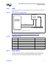
5.1 DRAM
For DDR SDRAM Sizes and Configurations, see section 7.2.2.1, table 139 of theIntel
®
80219
General Purpose PCI Processor Developer’s Manual. Table 89 provides DDR SDRAM Address
Register Definitions, while this sections also contains multiple examples of Address Register
Programming.
See the Intel
®
80219 General Purpose PCI Processor Design Guide, section 7.1, table 16 for
supported DDR and SDRAM configurations.
The Intel
®
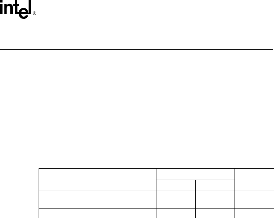
80219 general purpose PCI processor (80219) supports 2.5 V DDR memory. Table 88
lists the minimum/maximum values for the DDR memory bias voltages:
For all registers relating to DRAM and other MCU related registers, see section 7.6, Table 149 of the
Intel
®
80219 General Purpose PCI Processor Developer’s Manual.
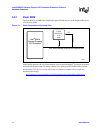
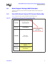
5.2 Components on the Peripheral Bus
The 80219 has a peripheral bus which contains the following peripheral devices:
• Flash ROM
• UART
• Rotary Switch
• Hex Display
Peripheral memory-Mapped Register Locations for the Peripheral Bus Interface Unit can be found in
the Intel
®
80219 General Purpose PCI Processor Developer’s Manual, Section 7.5, Table 298, sheet
7 of 12. The appropriate Base address and Limit registers must be set for each of the six chip enables
(PCE0-5). Each peripheral and its corresponding PCE# are described in this section.
All registers associated with the PBI can be found in the Intel
®
80219 General Purpose PCI
Processor Developer’s Manual, section 8.6, table 128.
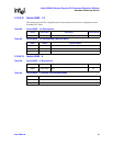
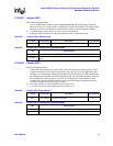
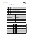
Table 88. DDR Memory Bias Voltage Minimum/Maximum Values
Symbol Parameter
Voltages
Units
Minimum Maximum
V
CC25
2.5 V Supply Voltage 2.3 2.7 V
V
REF
Memory I/O Reference Voltage 1.15 1.35 V
V
TT
DDR Memory Termination Voltage V
REF
- 0.04 V
REF
+ 0.04 V