


4 September, 2004 Document Number: 274069-001US
Intel
®
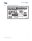
IQ80332 I/O Processor Evaluation Platform Board Manual
Contents
3.7.1 Console Serial Port................................................................................................35
3.7.2 JTAG Debug..........................................................................................................36
3.7.2.1 JTAG Port ..............................................................................................36
3.8 Board Reset Scheme..........................................................................................................37
3.9 Switches and Jumpers........................................................................................................38
3.9.1 Switch Summary....................................................................................................38
3.9.2 Default Switch Settings of S7A1- Visual................................................................38
3.9.3 Jumper Summary ..................................................................................................39
3.9.4 Connector Summary..............................................................................................39
3.9.5 General Purpose Input/Output Header..................................................................39
3.9.6 Detail Descriptions of Switches/Jumpers...............................................................40
3.9.6.1 Switch S1C2: 80332 Reset....................................................................40
3.9.6.2 Switch S6A1: BPCI-X Reset ..................................................................40
3.9.6.3 Switch S8A1: Rotary..............................................................................40
3.9.6.4 Switch S7A1...........................................................................................40
3.9.6.4.1 S7A1-1: PCI-X Bus A Speed Enable corresponding to signal
name PBI_AD340
3.9.6.4.2 S7A1-2: Reset IOP core corresponding to signal name
PBI_AD540
3.9.6.4.3 S7A1-3: Configration Cycle Enable corresponding to signal
name PBI_AD641
3.9.6.4.4 S7A1-4: PCI-X Bus B Speed Enable corresponding to signal
name PBI_AD1041
3.9.6.4.5 S7A1-5: PCI-X Bus B Hot-Plug Reset Disable corresponding
to signal name PBI_AD1141
3.9.6.4.6 Switch S7A1- 6: Hot Plug Capable Disabled corresponding to
signal name PBI_AD1541
3.9.6.4.7 Switch S7A1 - 7: SMBUS Manageability Address Bit 0 corre-
sponding to signal name PBI_AD1742
3.9.6.4.8 Switch S7A1 - 8: SMBUS Manageability Address Bit 3 corre-
sponding to signal name PBI_AD1842
3.9.6.4.9 Switch S7A1- 9:SMBUS Manageability Address Bit 2 corre-
sponding to signal name PBI_AD1742
3.9.6.4.10 Switch S7A1- 10: SMBUS Manageability Address Bit 1 corre-
sponding to signal name PBI_AD1642
3.9.6.5 Jumper J7D1: Flash bit-width ................................................................43
3.9.6.6 Jumper J1C1: JTAG Chain....................................................................43
3.9.6.7 Jumper J1D2: UART Control .................................................................43
3.9.6.8 Jumper J7B4: SMBus Header ...............................................................44
3.9.6.9 Jumper J9D3: Buzzer Volume Control...................................................44
4 Software Reference.....................................................................................................................45
4.1 DRAM .................................................................................................................................45
4.2 Components on the Peripheral Bus....................................................................................45
4.2.1 Flash ROM.............................................................................................................46
4.2.2 Peripheral Bus Memory Map.................................................................................47
4.3 Board Support Package (BSP) Examples ..........................................................................48
4.3.1 Intel
®
80332 I/O Processor Memory Map..............................................................48
4.3.2 RedBoot* Intel
®
80332 I/O Processor Memory Map .............................................49
4.3.3 RedBoot Intel
®
80332 I/O Processor Files ............................................................49
4.3.4 RedBoot 80332 DDR Memory Initialization Sequence..........................................50
A IQ80321 and IQ80332 Comparisons...........................................................................................51