


Timers
16-Bit Timer Setup Examples
MN102H75K/F75K/85K/F85K LSI User Manual Panasonic Semiconductor Development Company
101
Panasonic
4.11.3 Setting Up a Two-Phase PWM Output Signal Using
Timer 4
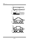
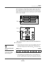
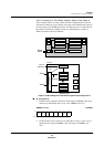
In this example, timer 4 is used to divide timer 0 underflow by 5 and generate a
five-cycle, two-phase PWM signal. The phase difference of this signal is 2
cycles. To accomplish this, the program must load the divide-by ratio of 5 (actual
setting: 4) into compare/capture register A and a cycle count of 2 (actual setting:
1) into compare/capture register B.
■
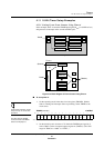
To set up the output port:
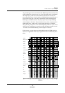
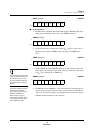
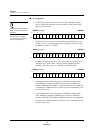
Set the P2MD[13:12] bits of the port 2 output mode register (P2MD) to b’01’
(selecting the TM4IOA pin), set the P2MD[11:10] bits to b’01’ (selecting the
TM4IOB pin), and set the P2DIR[6:5] bits of the port 2 I/O control register
(P2DIR) to b’11’ (selecting output direction). This step selects the TM4OA (P26)
and TM4OB (P25) pins as the timer output ports.
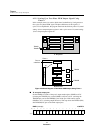
P2MD (example) x’00FFF4’
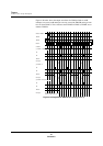
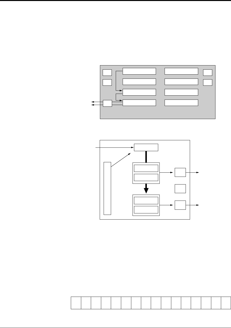
A. Chip Level
B. Block Level
Figure 4-32 Block Diagram of Two-Phase PWM Output Using Timer 4
TM4OA
TM4OB
P4
P5
CORE
Interrupts
Timers 0-3
Timers 4-5
ROM, RAM
Bus Controller
Serial I/Fs
ADC
P3
P6
P2
Timer 0
underflow
up
TM4BC
Timer 4
TM4CA
TM4CAX
TM4CB
TM4CBX
TM4OA
TM4OB
TQ
TQ
R
S
Q
Controller
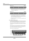
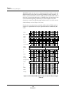
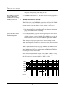
Bit:1514131211109876543210
—
P2
MD14
P2
MD13
P2
MD12
P2
MD11
P2
MD10
P2
MD9
P2
MD8
P2
MD7
P2
MD6
P2
MD5
P2
MD4
P2
MD3
P2
MD2
P2
MD1
P2
MD0
Setting:0001010000000000