


General Description
MN102H Series Description
MN102H75K/F75K/85K/F85K LSI User Manual Panasonic Semiconductor Development Company
23
Panasonic
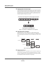
■ Internal registers, memory, and special function registers
Note: 1. This allocation is a representative example. Actual memory, peripheral, SFR, and I/O port configuration depends
on the product.
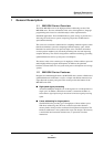
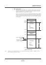
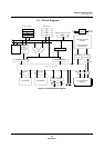
Figure 1-4 Internal Registers, Memory, and Special Function Registers
PC
023
A0
023
A1
A2
A3
D0
023
D1
D2
D3
MDR
015
PSW
015
ROM
RAM
CPUM, EFCR, IAGR
NMICR, xxICR
SCCTRn, TRXBUFn, SCSTRn
ANCTR, ANnBUF
TMn, BCn, BRn, ...
MEMMD
PnOUT, PnIN, PnDIR
Program Counter
Address Registers
Data Registers
Multiplication/Division Register
Processor Status Word
Memory, SFRs, and I/O Ports
The program counter specifies the 24-bit address of the
program instruction being executed.
The four address registers specify the location of the data in
the memory. A3 is assigned as the stack pointer.
The four data registers handle all arithmetic and logic
operations. When byte-length (8-bit) or word-length (16-bit)
data is to be transferred to memory or to another register, an
instruction adds a zero or sign extension.
The dedicated multiplication/division register stores the high-
order 16 bits of the 32-bit product of multiplication operations.
In division operations, before execution it stores the high-order
16 bits of the 32-bit dividend, and after execution it stores the
16-bit remainder of the quotient.
Memory (ROM and RAM), special function registers for
controlling peripheral functions, and I/O ports can all be
assigned to the same address space.
Internal control registers
1
Interrupt control registers
1
Serial interface registers
1
A/D converter registers
1
Timer/counter registers
1
Memory control registers
1
I/O port registers
1