


Chapter 1 Introduction
© National Instruments Corporation 1-3 R Series Intelligent DAQ User Manual
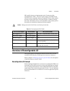
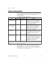
PXI-specific features are implemented on the J2 connector of the
CompactPCI bus. Table 1-2 lists the J2 pins used by the NI PXI-78xxR.
The NI 78xxR is compatible with any CompactPCI chassis with a sub-bus
that does not drive these lines. Even if the sub-bus is capable of driving
these lines, the R Series device is still compatible as long as those pins on
the sub-bus are disabled by default and are never enabled.
Caution Damage can result if the J2 lines are driven by the sub-bus.
Overview of Reconfigurable I/O
This section explains reconfigurable I/O and describes how to use the
LabVIEW FPGA Module to build high-level functions in hardware.
Refer to Chapter 2, Hardware Overview of the NI 78xxR, for descriptions
of the I/O resources on the NI 78xxR.
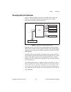
Reconfigurable I/O Concept
R Series Intelligent DAQ devices are based on a reconfigurable FPGA core
surrounded by fixed I/O resources for analog and digital input and output.
You can configure the behavior of the reconfigurable FPGA to match the
requirements of the measurement and control system. You can implement
this user-defined behavior as an FPGA VI to create an application-specific
I/O device.
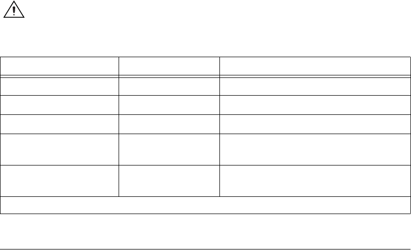
Table 1-2. Pins Used by the NI PXI-78xxR
NI PXI-78xxR Signal PXI Pin Name PXI J2 Pin Number
PXI Trigger<0..7> PXI Trigger<0..7> A16, A17, A18, B16, B18, C18, E16, E18
PXI Clock 10 MHz PXI Clock 10 MHz E17
PXI Star Trigger PXI Star Trigger D17
LBLSTAR<0..12>
*
LBL<0..12> A1, A19, C1, C19, C20, D1, D2, D15, D19,
E1, E2, E19, E20
LBR<0..12>
*
LBR<0..12> A2, A3, A20, A21, B2, B20, C3, C21,
D3, D21, E3, E15, E21
*
NI PXI-781xR/783xR only