


PBLS4004D_3 © NXP B.V. 2009. All rights reserved.
Product data sheet Rev. 03 — 6 January 2009 10 of 15
NXP Semiconductors
PBLS4004D
40 V PNP BISS loadswitch
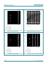
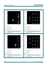
V
CE
=5V
(1) T
amb
= 150 °C
(2) T
amb
=25°C
(3) T
amb
= −40 °C
I
C
/I
B
=20
(1) T
amb
= 100 °C
(2) T
amb
=25°C
(3) T
amb
= −40 °C
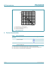
Fig 13. TR2 (NPN): DC current gain as a function of
collector current; typical values
Fig 14. TR2 (NPN): Collector-emitter saturation
voltage as a function of collector current;
typical values
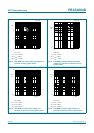
V
CE
= 0.3 V
(1) T
amb
= −40 °C
(2) T
amb
=25°C
(3) T
amb
= 100 °C
V
CE
=5V
(1) T
amb
= −40 °C
(2) T
amb
=25°C
(3) T
amb
= 100 °C
Fig 15. TR2 (NPN): On-state input voltage as a
function of collector current; typical values
Fig 16. TR2 (NPN): Off-state input voltage as a
function of collector current; typical values
I
C
(mA)
10
−1
10
2
101
006aaa038
10
2
10
10
3
h
FE
1
(1)
(2)
(3)
006aaa039
I
C
(mA)
110
2
10
10
−1
V
CEsat
(V)
10
−2
(1)
(2)
(3)
006aaa040
I
C
(mA)
10
−1
10
2
101
1
10
V
I(on)
(V)
10
−1
(1)
(2)
(3)
006aaa041
I
C
(mA)
10
−2
10
1
110
−1
1
10
V
I(off)
(V)
10
−1
(1)
(3)
(2)