


PBLS4004D_3 © NXP B.V. 2009. All rights reserved.
Product data sheet Rev. 03 — 6 January 2009 2 of 15
NXP Semiconductors
PBLS4004D
40 V PNP BISS loadswitch
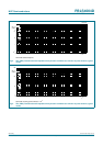
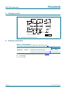
2. Pinning information
3. Ordering information
4. Marking
5. Limiting values
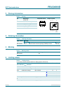
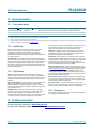
Table 2. Pinning
Pin Description Simplified outline Graphic symbol
1 emitter TR1
2 base TR1
3 output (collector) TR2
4 GND (emitter) TR2
5 input (base) TR2
6 collector TR1
132
4
56
65 4
1
23
R2
TR1
TR2
R1
sym036
Table 3. Ordering information
Type number Package
Name Description Version
PBLS4004D SC-74 plastic surface-mounted package (TSOP6); 6 leads SOT457
Table 4. Marking codes
Type number Marking code
PBLS4004D R4
Table 5. Limiting values
In accordance with the Absolute Maximum Rating System (IEC 60134).
Symbol Parameter Conditions Min Max Unit
TR1; PNP low V
CEsat
transistor
V
CBO
collector-base voltage open emitter - −40 V
V
CEO
collector-emitter voltage open base - −40 V
V
EBO
emitter-base voltage open collector - −5V
I
C
collector current
[1]
- −0.7 A
[2]
- −0.85 A
[3]
- −1A
I
CM
peak collector current single pulse; t
p
≤ 1ms - −2A
I
B
base current - −0.3 A
I
BM
peak base current single pulse; t
p
≤ 1ms - −1A