


PBLS4004D_3 © NXP B.V. 2009. All rights reserved.
Product data sheet Rev. 03 — 6 January 2009 3 of 15
NXP Semiconductors
PBLS4004D
40 V PNP BISS loadswitch
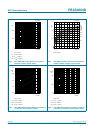
[1] Device mounted on an FR4 PCB, single-sided copper, tin-plated and standard footprint.
[2] Device mounted on an FR4 PCB, single-sided copper, tin-plated, mounting pad for collector 1 cm
2
.
[3] Device mounted on a ceramic PCB, Al
2
O
3
, standard footprint.
P
tot
total power dissipation T
amb
≤ 25 °C
[1]
- 250 mW
[2]
- 350 mW
[3]
- 400 mW
TR2; NPN resistor-equipped transistor
V
CBO
collector-base voltage open emitter - 50 V
V
CEO
collector-emitter voltage open base - 50 V
V
EBO
emitter-base voltage open collector - 10 V
V
I
input voltage
positive - +40 V
negative - −10 V
I
O
output current - 100 mA
I
CM
peak collector current single pulse; t
p
≤ 1 ms - 100 mA
P
tot
total power dissipation T
amb
≤ 25 °C - 200 mW
Per device
P
tot
total power dissipation T
amb
≤ 25 °C
[1]
- 400 mW
[2]
- 530 mW
[3]
- 600 mW
T
j
junction temperature - 150 °C
T
amb
ambient temperature −65 +150 °C
T
stg
storage temperature −65 +150 °C
Table 5. Limiting values
…continued
In accordance with the Absolute Maximum Rating System (IEC 60134).
Symbol Parameter Conditions Min Max Unit