


PBLS4004D_3 © NXP B.V. 2009. All rights reserved.
Product data sheet Rev. 03 — 6 January 2009 4 of 15
NXP Semiconductors
PBLS4004D
40 V PNP BISS loadswitch
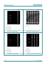
6. Thermal characteristics
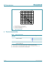
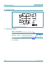
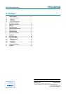
[1] Device mounted on an FR4 PCB, single-sided copper, tin-plated and standard footprint.
[2] Device mounted on an FR4 PCB, single-sided copper, tin-plated, mounting pad for collector 1 cm
2
.
[3] Device mounted on a ceramic PCB, Al
2
O
3
, standard footprint.
(1) Ceramic PCB, Al
2
O
3
, standard footprint
(2) FR4 PCB, mounting pad for collector 1 cm
2
(3) FR4 PCB, standard footprint
Fig 1. Power derating curves
T
amb
(°C)
0 16012040 80
006aaa461
0.4
0.2
0.6
0.8
P
tot
(W)
0
(1)
(2)
(3)
Table 6. Thermal characteristics
Symbol Parameter Conditions Min Typ Max Unit
Per device
R
th(j-a)
thermal resistance from
junction to ambient
in free air
[1]
- - 312 K/W
[2]
- - 236 K/W
[3]
- - 210 K/W
Per TR1; PNP low V
CEsat
transistor
R
th(j-sp)
thermal resistance from
junction to solder point
- - 105 K/W