


Philips Semiconductors Product specification
PTN3501Maintenance and control device
2001 Jan 17
10
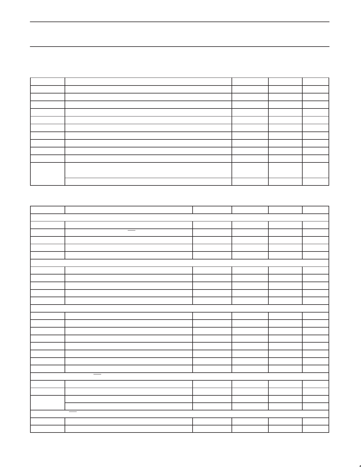
ABSOLUTE MAXIMUM RATINGS
Absolute Maximum Ratings are those values beyond which damage to the device may occur. Functional operation under these conditions is not implied.
SYMBOL
PARAMETER MIN MAX UNIT
V
CC
Supply Voltage –0.5 4.0 V
V
I
Input Voltage V
SS
– 0.5 5.5 V
I
I
DC Input Current –20 20 mA
I
O
DC Output Current –25 25 mA
I
DD
Supply Current –100 100 mA
I
SS
Supply Current –100 100 mA
P
tot
Total Power Dissipation – 400 mW
P
O
Total Power Dissipation per Output – 100 mW
T
STG
Storage Temperature –65 +150
_C
T
AMB
Operating Temperature –40 +85
_C
V
ESD
Electrostatic Discharge:
Human Body Model, 1.5 kΩ, 100 pF – >2000 V
Machine Model, 0 Ω, 200 pF – >200 V
DC ELECTRICAL CHARACTERISTICS
T
amb
= –40_C to +85_C unless otherwise specified; V
CC
= 3.3 V
SYMBOL PARAMETER MIN TYP MAX UNIT
Supply
V
DD
Supply Voltage 2.5 3.3 3.6 V
I
DDQ
Standby Current; A
0
thru A
5
, WC = HIGH – 60 µA
I
DD1
Supply Current Read – – 1 mA
I
DD2
Supply Current Write – – 2 mA
V
POR
Power on Reset Voltage – – 2.4 V
Input SCL; input, output SDA
V
IL
Input LOW voltage –0.5 – 0.3 V
DD
V
V
IH
Input HIGH voltage 0.7 V
DD
– 5.5 V
I
OL
Output LOW current @ V
OL
= 0.4 V 3 – – mA
I
L
Input leakage current @ V
I
= V
DD
or V
SS
–1 – 1 µA
C
I
Input capacitance @ V
I
= V
SS
– – 7 pF
I/O Expander Port
V
IL
Input LOW voltage –0.5 – 0.3 V
DD
V
V
IH
Input HIGH voltage 0.7 V
DD
– 5.5 V
I
IHL(max)
Input current through protection diodes –400 – 400 µA
I
OL
Output LOW current @ V
OL
= 1 V 10 25 – mA
I
OH
Output HIGH current @ V
OH
= V
ss
30 100 300 µA
I
OHt
Transient pull–up current – 2 – mA
C
I
Input Capacitance – – 10 pF
C
O
Output Capacitance – – 10 pF
Address Inputs A
0
thru A
5
, WC input
V
IL
Input LOW voltage –0.5 – 0.3 V
DD
V
V
IH
Input HIGH voltage 0.7 V
DD
– 5.5 V
I
L
Input leakage current @ V
I
= V
DD
–1 – 1 µA
Input leakage (pull-up) current @ V
I
= V
SS
10 25 100 µA
Interrupt output INT
I
OL
Low level output current; V
OL
= 0.4 V 1.6 – – mA
I
L
Leakage current @ V
I
= V
DD
or V
SS
–1 – +1 µA