1998 Feb 16 30
Philips Semiconductors Product specification
CMOS digital decoding IC with RAM for
Compact Disc
SAA7345
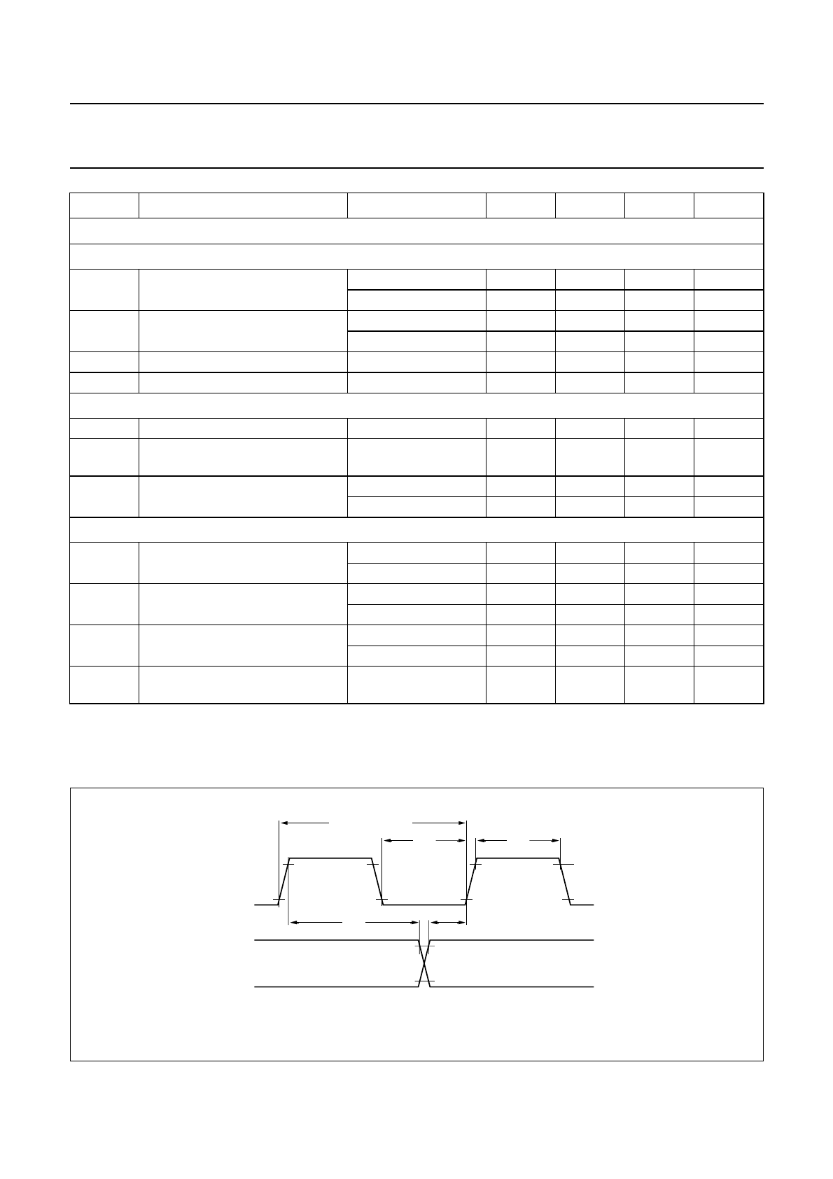
Notes
1. Timing reference voltage levels are 0.8 V and V
DD
− 0.8 V.
2. Negative set-up time means that data may change after clock transition.
Microcontroller interface timing (see Figs 24 and 25)
I
NPUTS CL AND RAB
t
L
input LOW time single speed 500 −−ns
double speed 260 −−ns
t
H
input HIGH time single speed 500 −−ns
double speed 260 −−ns
t
r
rise time single speed −−480 ns
t
f
fall time double speed −−240 ns
R
EAD MODE
t
dRD
delay time RAB to DA valid 0 − 50 ns
t
dRZ
delay time RAB to DA
high-impedance
0 − 50 ns
t
pd
propagation delay CL to DA single speed 700 − 980 ns
double speed 340 − 500 ns
W
RITE MODE
t
suD
set-up time DA to CL single speed; note 2 −700 −−ns
double speed; note 2 −340 −−ns
t
hD
hold time CL to DA single speed −−980 ns
double speed −−500 ns
t
suCR
set-up time CL to RAB single speed 260 −−ns
double speed 140 −−ns
t
dWZ
delay time DA high-impedance
to RAB
50 −−ns
SYMBOL PARAMETER CONDITIONS MIN. TYP. MAX. UNIT
Fig.23 I
2
S timing.
DD
V – 0.8 V
0.8 V
DD
V – 0.8 V
0.8 V
t
H
MGA376 - 1
t
L
clock period t
cy
SCLK
WCLK
DATA
MISC
t
h
t
su


