12 Configuration Register
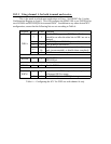
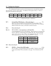
The Configuration Register is used to set the interrupt source and enable the interface
between the SCC and the external FIFOs. The address of this register is Base+5. Table 10
details the bit definitions of the register.
0RXSRCFIFOEN0INTS0INTS101
Bit 0Bit 1Bit 2Bit 3Bit 4Bit 5Bit 6Bit 7
Table 10 --- Configuration Register - Read/Write
Bit 7: External Data FIFOs Present --- Reserved, always 1. This
bit can be used as an indicator that external data FIFOs are present. Other
MPA-series products that are not equipped with external data FIFOs, including
MPAP-100 Revision A cards, will return 0 in this bit location.
Bit 6: Reserved, always 0.
Bits 5-4: INTS1, INTS0 --- Interrupt Source and Enable Bits: These
two bits determine the source of the interrupt. The two sources are interrupt from
the SCC (INTSCC), and interrupt on Test Mode (INTTM). Only one interrupt
source can be active at a time. Below is the mapping for these bits. Note that
FIFO-related interrupts will occur only when INTSCC is chosen.
INTTM11
INTSCC01
reserved00
Interrupts disabled00
Interrupt SourceINTS0INTS1
Bit 3: Reserved, always 0.
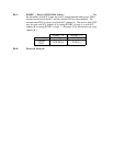
Bit 2: FIFOEN --- External data FIFO enable: If this
bit is set (logic 1), the external data FIFOs are enabled. If this bit is clear (logic
0), the external data FIFOs are disabled. (See page 31 for full details on FIFO
use.)


