


14
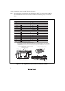
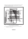
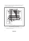
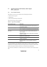
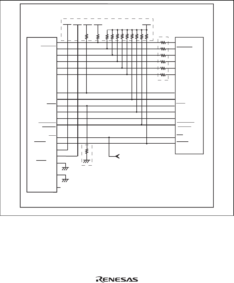
When the circuit is connected as shown in figure 1.7, the switches of the emulator are set as SW2
= 1 and SW3 = 1. For details, refer to section 3.8, Setting the DIP Switches, in the SuperH
TM
Family E10A-USB Emulator User’s Manual.
6
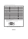
AUDATA0
AUDATA2
AUDATA1
AUDATA3
TCK
TMS
AUDSYNC
RES
TDI
TDO
TRST
ASEBRKAK
/ASEBRK
UVCC
UVCC_AUD
ASEMD (GND)
32
30
28
26
24
15
17
21
19
11
8
9
3
14
12
UCON (GND)
5
1, 2, 4, 7,
10, 13, 16, 18,
20, 22, 23, 25, 27, 29,
31, 33, 34, 35, 36, 37, 38
AUDATA0
AUDATA2
AUDATA1
AUDATA3
TCK
RES
TMS
TDO
TDI
TRST
ASEBRKAK
/ASEBRK
AUDCK
AUDSYNC
AUDCK
N.C.
PVcc
ASEMD
PVccPVcc
PVcc
PVcc
GND
GND bus leads
SoC
User system
Reset signal
PVcc = I/O power supply
H-UDI port connector
(38-pin type)
Figure 1.7 Recommended Circuit for Connection between the H-UDI Port Connector and
MCU when the Emulator is in Use (38-Pin Type)
Note: For the pin names of MCUs and recommended circuits for connection, ask Renesas
Technology Corp. via the sales office.