RV5VH1××/RV5VH2××
16
DC/DC Converter 2
*
) VOUT1=5.0V, VOUT2=–3.0V, IOUT2=1mA : unless otherwise specified. (See Typical Application)
*
1 ) Adjustable by external resistors to -30V.
*
2 ) “Minimum Operating Voltage”means a voltage for the “VOUT1” pin.
*
3 ) This value shows only the supply current of DC/DC2, not include the supply current of external resistors.
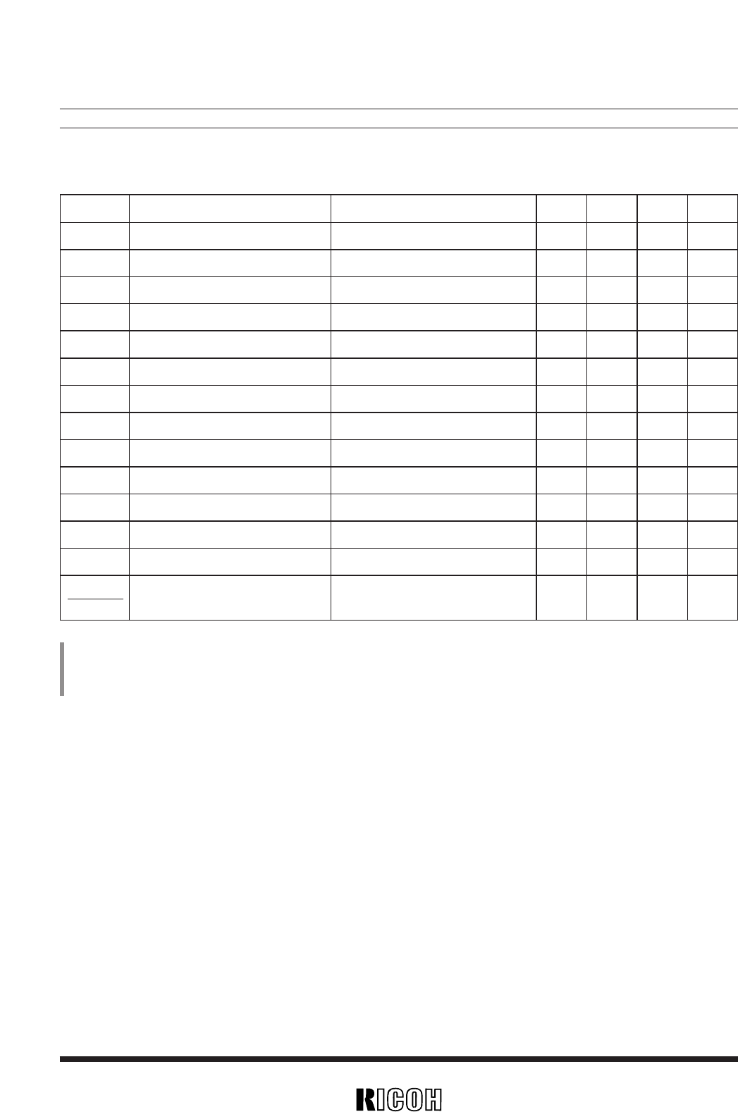
Symbol Item Conditions MIN. TYP. MAX. Unit
VSET Output Voltage Setting Range *
1
0 V
VFB Feed Back Voltage 0 mV
VIN Maximum Input Voltage 10 V
VOPTmin Minimum Operating Voltage*
2
IOUT=1mA 1.8 V
ISS2 Supply Current2*
3
CSW= “H”, No Load 25 µA
Istandby Standby Current CSW=“L” 0.3 µA
IEXT2H EXT2 “H” Output Current VEXT2=VOUT1–0.4V 3 6 mA
IEXT2L EXT2 “L” Output Current VEXT2=0.4V 7 14 mA
fosc Maximum Oscillator Frequency 110 130 150 kHz
Maxdty Oscillator Duty Cycle VEXT2=“H” 40 50 60 %
VCSWH CSW “H” Input Voltage VOUT1=5.0V 1.6 VOUT1 V
VCSWL CSW “L” Input Voltage VOUT1=5.0V 0 0.4 V
ICSWleak CSW Input Leakage Current CSW=5.0V –0.5 0.5 µA
∆V
FB
Feed Back Voltage Temp.Co. –40˚C≤Topt≤85˚C ±30 µV/˚C
∆Topt
VOUT1=5.0V, Topt=25˚C


