


RV5VH3××
38
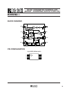
OPERATION
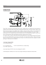
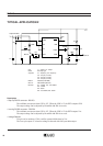
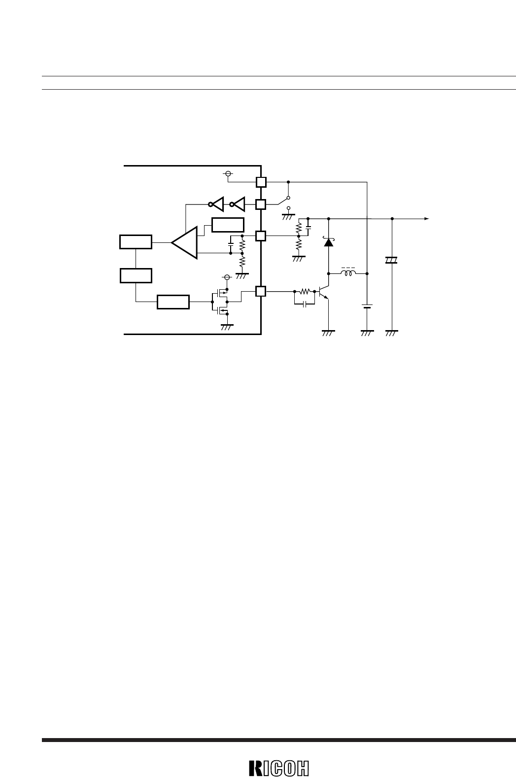
• DC/DC Converter 1
The DC/DC1 can operate by an input voltage to the V
DD pin. A change in the VOUT1 will feed back to the internal error
amplifier through external voltage setting resistors and internal feed back resistors. When the feed back voltage is lower
than the reference voltage the error amplifier enables oscillation or otherwise will stop oscillation. The internal feed back
resistor “R” which is fixed and adjusted by laser trim can make the feed back input voltage to “Error Amp.1” stable.
Pulses from the “OSC” circuit have a duty cycle of 50% and it becomes 65 to 75%(at high side) through the “P_shift” circuit.
These clock pulses control VFM circuit and make it possible to operate as a boost converter.
The output of “EXT1” is driven by CMOS buffer and an external NMOS driver is also available instead of an NPN transis-
tor, in such cases the Rb and Cb are not necessary. The DC/DC1 can be shut down by CSW pin. When the CSW pin is
High, V
DD level, the DC/DC1 is enabled and when the CSW pin is Low, GND level, the DC/DC1 is disabled. The EXT1
pin outputs “L” while the DC/DC1 is disabled.
• Set Output Voltage DC/DC1
V
OUT1 is described as follows :
V
OUT1 : R1+R2=VFB1 : R2 DC/DC1 controls VFB1 to be a constant voltage
V
OUT1=VFB1 × (R1+R2) / R2
so any output voltage of DC/DC1 can be set by changing R1 or/and R2.
Certain temperature coefficient of V
OUT1 can be set by using R1, R2 having such temperature characteristics.
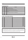
FB1
EXT1
+
–
RV5VH3××
Error Amp.1
VFM1
CSW
4
1
2
OSC
R2
R1
p_shift
C
L1
SBD
V
OUT1
VIN
NPN Tr.
Cb
Rb
3
Vref
VDD