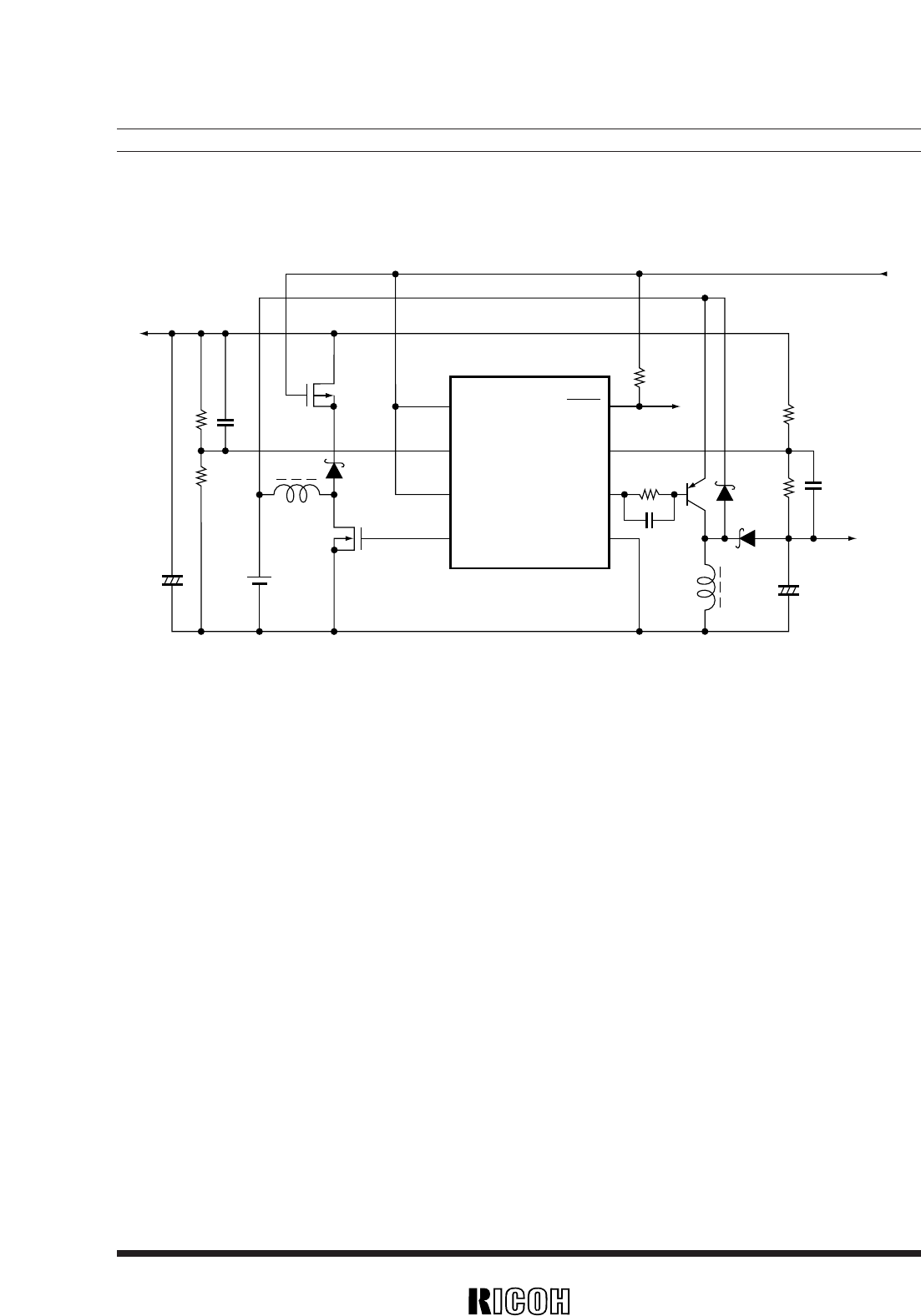
43
RV5VH3××
CSW
FB1
V
DD
EXT1
D
OUT
FB2
EXT2
GND
C2
L2
R3
R1
R2
C3
SBD3
C1
PNP Tr.
SBD1
R6
R5
C5
L1
R4
C4
NMOS
PMOS
VIN
SBD2
Output DC/DC 2
Output DC/DC 1
R1 : 820kΩ, R2 : 820kΩ, R3 : 100kΩ, R4 : 1kΩ, R5 : 750kΩ (AdjustabIe)
R6 : 100kΩ
L1 : 68µH, L2 : 27µH
C1 : 22µF, C2 : 22µF, C3 : 1000pF, C4 : 2200pF, C5 : 1000pF
PMOS : 2SJ238, NMOS : 2SK1470, PNPTr. : 2SB1120F
Operation
The V
DD voltage can be supplied from another source than battery output and a reference voltage for DC/DC2 is
supplied by the output of DC/DC1.
The PMOS transistor can operate as a switch when the CSW is “L”.
• Step up DC/DC converter : DC/DC1
The oscillator can operate when CSW is “H”. When the CSW is “L” the EXT1 outputs GND.
The output voltage can be adjusted by R5 and R6 with FB1 of two volt.
• Invering DC/DC converter : DC/DC2
The oscillator can operate when CSW is “H”. When the CSW is “L” the EXT2 outputs V
DD.
The output voltage can be adjusted by R1 and R2 with FB2 of zero volt.
• VoItage Detector
V
DD pin can be monitored. This could be operated all the time by VDD.
The D
OUT pin outputs “L” when low voltage is detected with Nch open-drain output.
TYPICAL APPLICATION 3


