


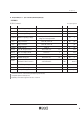
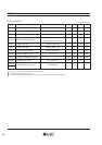
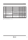
39
RV5VH3××
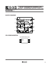
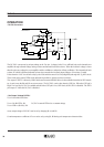
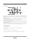
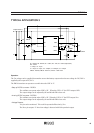
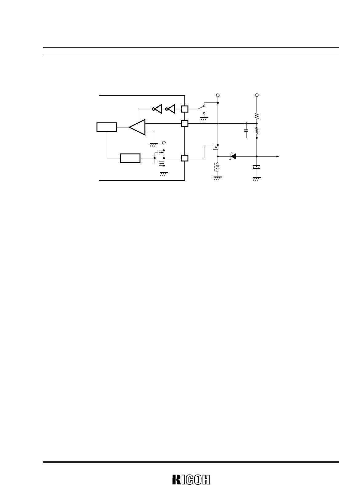
• DC/DC Converter 2
The DC/DC2 can operate by an input voltage to the V
DD pin. A change in the VOUT2 will feed back to the internal error
amplifier through external voltage setting resistors. The V
REF voltage should be provided from externally fixed power sup-
ply such as V
OUT1.
When the feed back voltage to the Error Amp.2 is higher than the ground voltage the error amplifier enables oscillation or
otherwise will stop oscillation.
Pulses from the “OSC” circuit have a duty cycle of 50% and it makes VFM operation allowable.
There might be certain cases that the duty cycles becomes smaller temporally at light load current. The output of “EXT2”
is driven by CMOS buffer operated V
DD and GND.
A PMOS driver will be connected to the “EXT2” pin and its switching operation generates negative output voltage through
energy accumulated in an inductor.
The DC/DC1 can be shut down by CSW pin. When the CSW pin is High, V
DD
level, the DC/DC1 is enabled and when the
CSW pin is Low, GND level, the DC/DC1 is disabled. The EXT2 pin outputs High while the DC/DC2 is disabled.
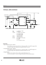
• Set Output Voltage DC/DC 2
V
OUT2 is described as follows:
V
REF : R1=|–VOUT2| : R2 The FB2 voltage is controlled to 0V and VREF is provided externally
|–V
OUT2|=VREF×R2/R1
so any output voltage of DC/DC2 can be set by changing R1 or/and R2.
Certain temperature coefficient of V
OUT2 can be set by using R1, R2 having such temperature characteristics.
C1
L
FB2
V
OUT2
VDD
EXT2
+
–
RV5VH3××
Error Amp.2
VFM2
CSW
6
1
7
SBD
+
PMOS
OSC
C2 R2
R1
VREF