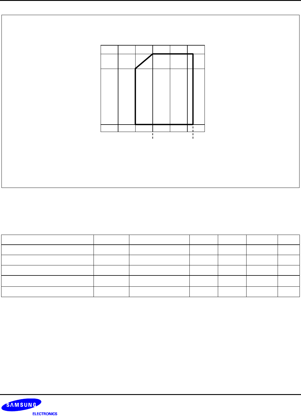
S3C8275X/F8275X/C8278X/F8278X/C8274X/F8274X ELECTRICAL DATA
17-13
2 MHz
6.25 kHz(main)/8.2 kHz(sub)
24
Supply Voltage (V)
Instruction Clock = 1/4n x oscillator frequency (n = 1, 2, 8, 16)
1.05 MHz
Instruction Clock
8 MHz
4.2 MHz
fx (Main/Sub oscillation frequency)
2.5 3.6
400 kHz (main)/32.8 kHz(sub)
3
1
Figure 17-9. Operating Voltage Range
Table 17-12. A.C. Electrical Characteristics for Internal Flash ROM
(T
A
= − 25
°
C to + 85
°
C, V
DD
= 2.2 V to 3.6 V)
Parameter Symbol Conditions Min Typ Max Unit
Programming time
(1)
Ftp
−
30
− − µs
Chip erasing time
(2)
Ftp1
−
50
− −
ms
Sector erasing time
(3)
Ftp2
−
10
− −
ms
Data access time
Ft
RS
− −
25
−
ns
Number of writing/erasing FNwe
− − −
10,000
(4)
Times
NOTES:
1. The programming time is the time during which one byte (8-bit) is programmed.
2. The chip erasing time is the time during which all 16K byte block is erased.
3. The sector erasing time is the time during which all 128 byte block is erased.
4. Maximum number of writing/erasing is 10,000 times for full-flash(S3F8275X) and 100 times for half-flash
(S3F8278X/F8274X).
5. The chip erasing is available in Tool Program Mode only.


