


ADDRESSING MODES S3C8275X/F8275X/C8278X/F8278X/C8274X/F8274X
3-6
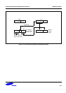
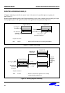
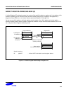
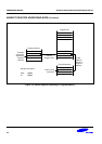
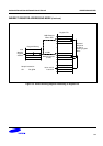
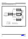
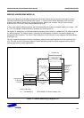
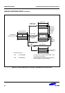
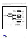
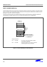
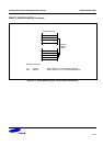
INDIRECT REGISTER ADDRESSING MODE (Concluded)
dst
OPCODE
4-bit Working
Register Address
Sample Instructions:
LCD R5,@RR6 ; Program memory access
LDE R3,@RR14 ; External data memory access
LDE @RR4, R8 ; External data memory access
Program Memory
Register File
src
Value used in
Instruction
OPERAND
Example Instruction
References either
Program Memory or
Data Memory
Program Memory
or
Data Memory
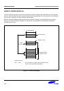
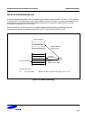
Next 2-bit Point
to Working
Register Pair
(1 of 4)
LSB Selects
Register
Pair
16-Bit
address
points to
program
memory
or data
memory
RP0 or RP1
MSB Points to
RP0 or RP1
Selected
RP points
to start of
working
register
block
Figure 3-6. Indirect Working Register Addressing to Program or Data Memory