


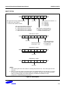
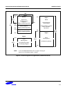
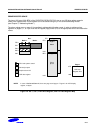
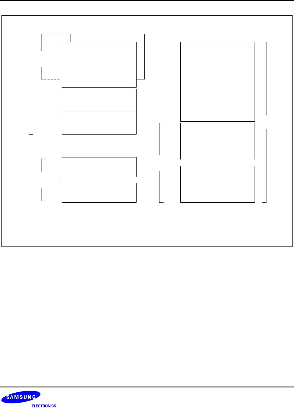
S3C8275X/F8275X/C8278X/F8278X/C8274X/F8274X ADDRESS SPACES
2-7
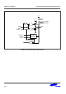
System Registers
(Register Addressing Mode)
General Purpose Register
(Register Addressing Mode)
Bank 1
System and
Peripheral Control
Registers
Bank 0
System and
Peripheral Control
Registers
(Register Addressing Mode)
Set1
FFH
E0H
32
Bytes
E0H
DFH
D0H
CFH
C0H
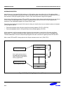
Prime
Data Registers
(All addressing modes)
LCD Display Reigster
~ ~
Page 2
0FH
00H
16
Bytes
~
Page 0
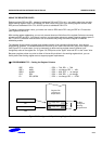
Prime
Data Registers
(All Addressing Modes)
Page 0
Set 2
General-Purpose
Data Registers
(Indirect Register, Indexed
Mode, and Stack
Operations)
~ ~
C0H
BFH
00H
FFH
192
Bytes
64
Bytes
256
Bytes
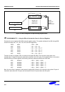
NOTE: In case of S3C8278X/C8274X, there are page 0 and page 2.
Page 2 is for LCD display register, 16 bytes.
Figure 2-4. Internal Register File Organization (S3C8278X/C8274X)