


- 4 -
Unbuffered SODIMM datasheet DDR3 SDRAM
Rev. 1.0
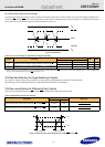
1. DDR3 Unbuffered SODIMM Ordering Information
NOTE :
1. "##" - F8/H9
2. F8 - 1066Mbps 7-7-7 & H9 - 1333Mbps 9-9-9
- DDR3-1333(9-9-9) is backward compatible to DDR3-1066(7-7-7)
2. Key Features
• JEDEC standard 1.5V ± 0.075V Power Supply
•V
DDQ
= 1.5V ± 0.075V
• 400 MHz f
CK
for 800Mb/sec/pin, 533MHz f
CK
for 1066Mb/sec/pin, 667MHz f
CK
for 1333Mb/sec/pin
• 8 independent internal bank
• Programmable CAS Latency: 5,6,7,8,9
• Programmable Additive Latency(Posted CAS) : 0, CL - 2, or CL - 1 clock
• Programmable CAS Write Latency(CWL) = 5(DDR3-800), 6(DDR3-1066) and 7(DDR3-1333)
• Burst Length: 8 (Interleave without any limit, sequential with starting address “000” only), 4 with tCCD = 4 which does not allow seamless read or
write [either On the fly using A12 or MRS]
• Bi-directional Differential Data Strobe
• On Die Termination using ODT pin
• Average Refresh Period 7.8us at lower then T
CASE
85°C, 3.9us at 85°C < T
CASE
≤ 95°C
• Asynchronous Reset
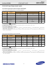
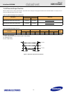
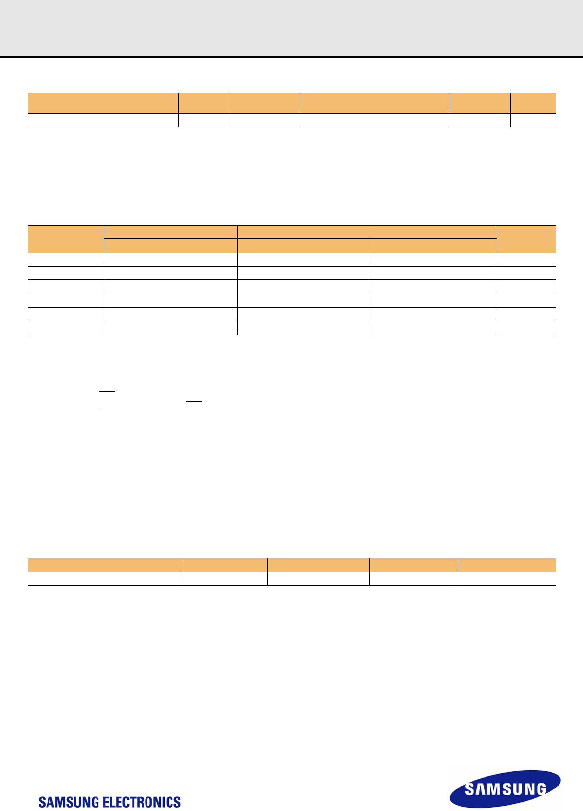
3. Address Configuration
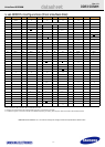
Part Number
2
Density Organization Component Composition
Number of
Rank
Height
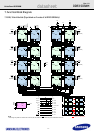
M471B1G73AH0-CF8/H9 8GB 1Gx64 512Mx8(K4B4G0846A-HC##)*16 2 30mm
Speed
DDR3-800 DDR3-1066 DDR3-1333
Unit
6-6-6 7-7-7 9-9-9
tCK(min) 2.5 1.875 1.5 ns
CAS Latency 6 79tCK
tRCD(min) 15 13.125 13.5 ns
tRP(min) 15 13.125 13.5 ns
tRAS(min) 37.5 37.5 36 ns
tRC(min) 52.5 50.625 49.5 ns
Organization Row Address Column Address Bank Address Auto Precharge
512Mx8(4Gb) based Module A0-A15 A0-A9 BA0-BA2 A10/AP