


- 7 -
Unbuffered SODIMM datasheet DDR3 SDRAM
Rev. 1.0
6. Input/Output Functional Description
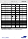
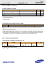
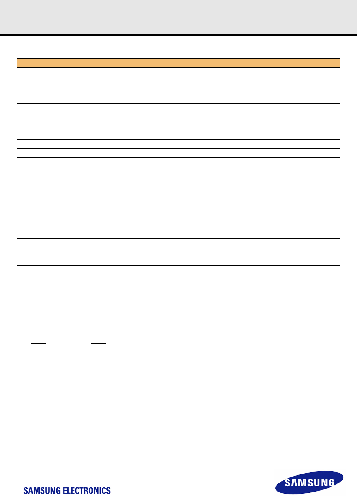
Symbol Type Function
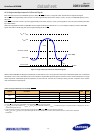
CK0-CK1
CK0
-CK1
Input
The system clock inputs. All address and command lines are sampled on the cross point of the rising edge of CK and
falling edge of CK. A Delay Locked Loop (DLL) circuit is driven from the clock inputs and output timing for read opera-
tions is synchronized to the input clock.
CKE0-CKE1 Input
Activates the DDR3 SDRAM CK signal when high and deactivates the CK signal when low. By deactivating the clocks,
CKE low initiates the Power Down mode or the Self Refresh mode.
S
0-S1 Input
Enables the associated DDR3 SDRAM command decoder when low and disables the command decoder when high.
When the command decoder is disabled, new commands are ignored but previous operations continue. Rank 0 is
selected by S
0; Rank 1 is selected by S1.
R
AS, CAS, WE Input
When sampled at the cross point of the rising edge of CK and falling edge of CK
, signals CAS, RAS, and WE define
the operation to be executed by the SDRAM.
BA0-BA2 Input Selects which DDR3 SDRAM internal bank of eight is activated.
ODT0-ODT1 Input Asserts on-die termination for DQ, DM, DQS, and DQS signals if enabled via the DDR3 SDRAM mode register.
A0-A9,
A10/AP,
A11
A12/BC
A13-A15
Input
During a Bank Activate command cycle, defines the row address when sampled at the cross point of the rising edge of
CK and falling edge of CK
. During a Read or Write command cycle, defines the column address when sampled at the
cross point of the rising edge of CK and falling edge of CK
. In addition to the column address, AP is used to invoke
autoprecharge operation at the end of the burst read or write cycle. If AP is high, autoprecharge is selected and BA0-
BAn defines the bank to be precharged. If AP is low, autoprecharge is disabled. During a Precharge command cycle,
AP is used in conjunction with BA0-BAn to control which bank(s) to precharge. If AP is high, all banks will be pre-
charged regardless of the state of BA0-BAn inputs. If AP is low, then BA0-BAn are used to define which bank to pre-
charge.A12(BC
) is sampled during READ and WRITE commands to determine if burst chop (on-the fly) will be
performed (HIGH, no burst chop; LOW, burst chopped)
DQ0-DQ63 I/O Data Input/Output pins.
DM0-DM7 Input
The data write masks, associated with one data byte. In Write mode, DM operates as a byte mask by allowing input
data to be written if it is low but blocks the write operation if it is high. In Read mode, DM lines have no effect.
DQS0-DQS7
DQS
0-DQS7
I/O
The data strobes, associated with one data byte, sourced with data transfers. In Write mode, the data strobe is
sourced by the controller and is centered in the data window. In Read mode, the data strobe is sourced by the DDR3
SDRAMs and is sent at the leading edge of the data window. DQS
signals are complements, and timing is relative to
the crosspoint of respective DQS and DQS
.
V
DD
,V
DDSPD,
V
SS
Supply Power supplies for core, I/O, Serial Presence Detect, Temp sensor, and ground for the module.
V
REFDQ,
V
REFCA
Supply Reference voltage for SSTL15 inputs.
SDA I/O
This is a bidirectional pin used to transfer data into or out of the SPD EEPROM and Temp sensor. A resistor must be
connected from the SDA bus line to V
DDSPD
on the system planar to act as a pull up.
SCL Input This signal is used to clock data into and out of the SPD EEPROM and Temp sensor.
SA0-SA1 Input Address pins used to select the Serial Presence Detect and Temp sensor base address.
TEST I/O The TEST pin is reserved for bus analysis tools and is not connected on normal memory modules
RESET
Input RESET In Active Low This signal resets the DDR3 SDRAM