


Si53xx-RM
106 Rev. 0.5
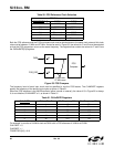
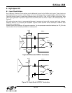
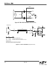
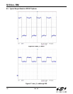
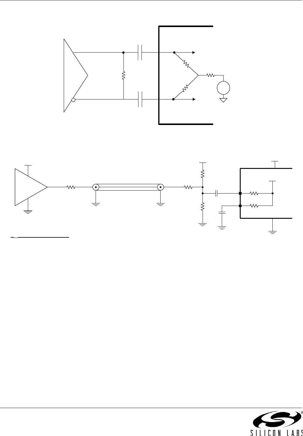
Figure 40. CML/LVDS Termination (1.8, 2.5, 3.3 V)
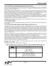
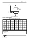
Figure 41. CMOS Termination (1.8, 2.5, 3.3 V)
40 k
C
C
±
CKIN
_
CKIN
+
V
ICM
300
100
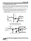
Si53xx
CML/
LVDS
Driver
40 k
V
DD
V
DD
V
DD
CMOS Driver
R1
33 ohms
50
R2
See Table
R3
150 ohms
C1
100 nF
R4
150 ohms
C2
100 nF
V
ICM
CKIN+
CKIN–
R5 40 kohm
R6 40 kohm
V
DD
R2 Notes
3.3 V 100 ohm Locate R1 near CMOS driver
2.5 V 49.9 ohm Locate other components near Si5317
1.8 V 14.7 ohm Recalculate resistor values for other drive strengths
Additional Notes:
1. Attenuation circuit limits overshoot and undershoot.
2. Not to be used with non-square wave input clocks.
Si53xx