


Si53xx-RM
108 Rev. 0.5
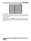
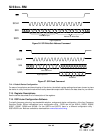
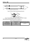
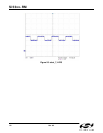
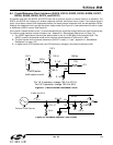
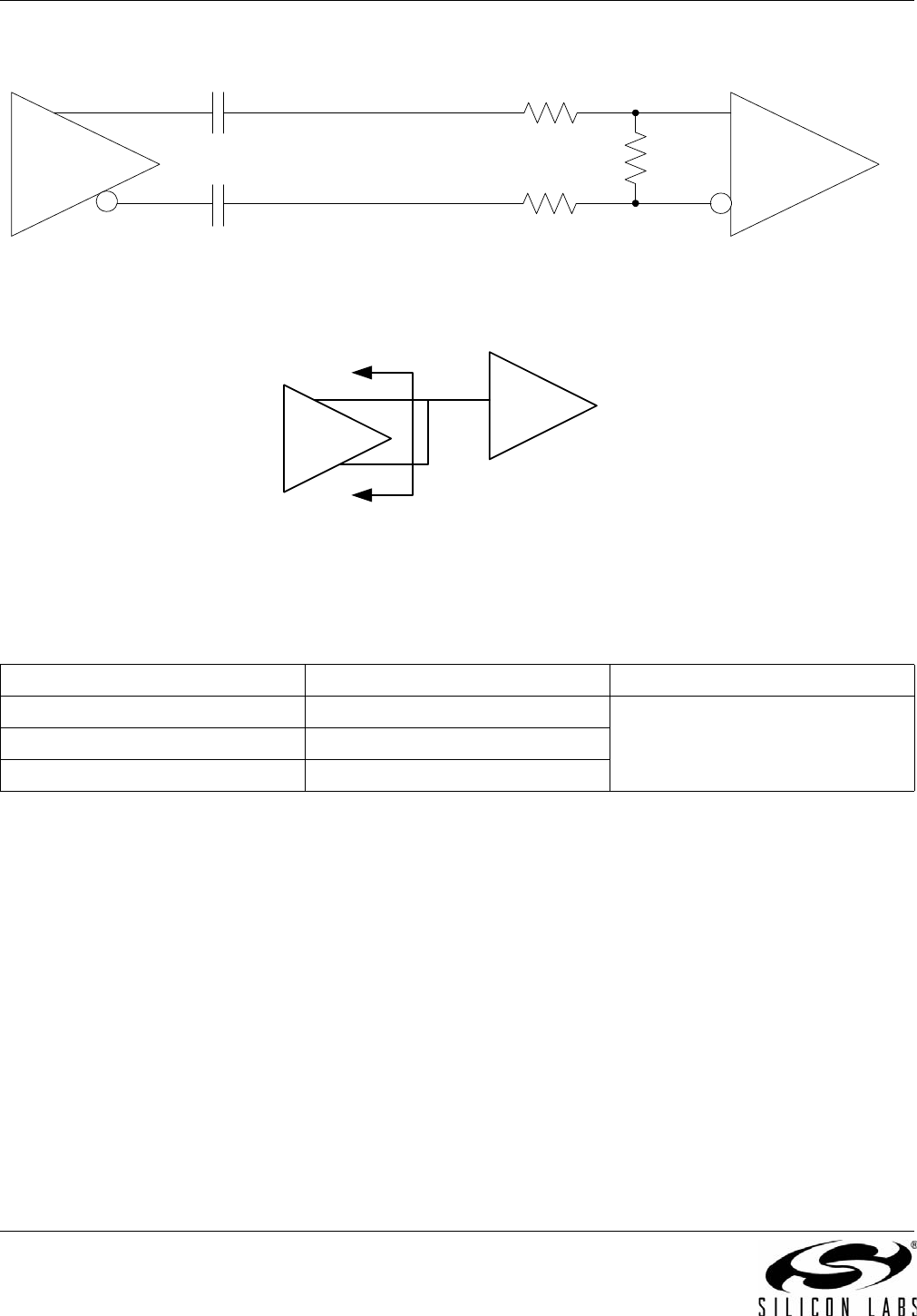
Figure 43. Differential Output Example Requiring Attenuation
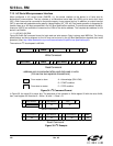
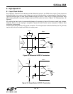
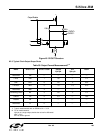
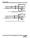
Figure 44. Typical CMOS Output Circuit (Tie CKOUTn+ and CKOUTn– Together)
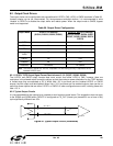
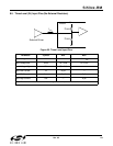
Unused output drivers should be powered down, per Table 57, or left floating.
The pin-controlled parts have a DBL2_BY pin that can be used to disable CKOUT2.
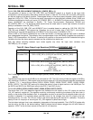
Table 57. Disabling Unused Output Driver
Output Driver Si5365, Si5366 Si5325, Si5326, Si5367, Si5368
CKOUT1 and CKOUT2 N/A Use SFOUT_REG to disable individ-
ual CKOUTn.
CKOUT3 and CKOUT4 DBL34
CKOUT5/FS_OUT DBL5/DBL_FS
Si53xx
Rcvr
10
10
80
All resistors are located next to RCVR
Si53xx
CMOS
Logic
CKOUTn
Optionally Tie CKOUTn
Outputs Together for Greater Strength