


Si53xx-RM
Rev. 0.5 15
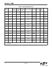
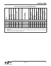
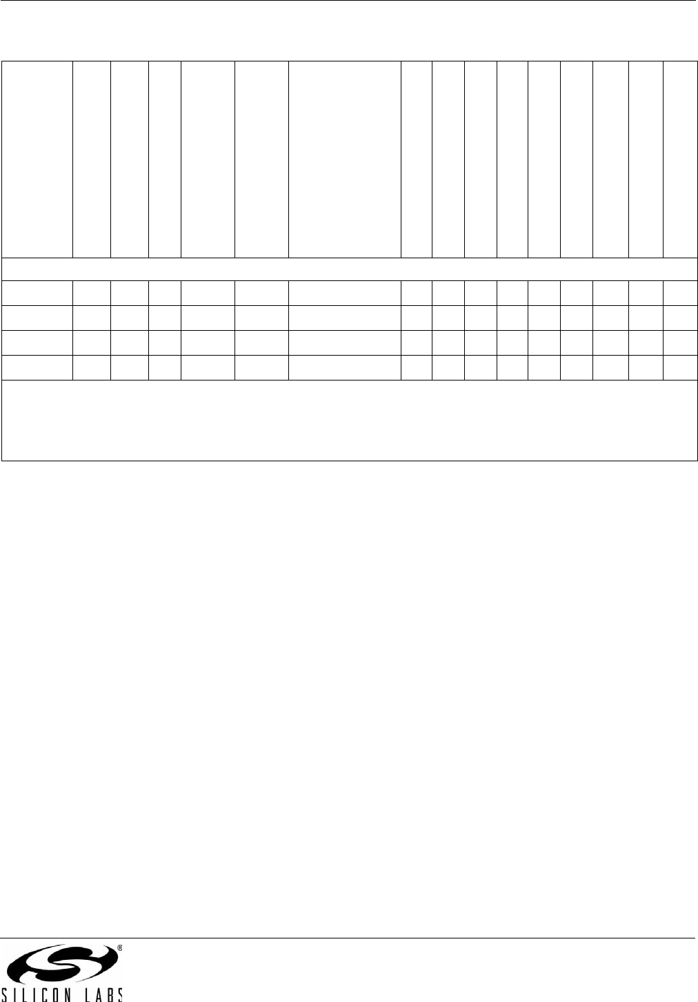
Table 2. Product Selection Guide (Si5322/25/65/67)
Device
Clock Inputs
Clock Outputs
P Control
Max Input Freq (MHz)
1
Max Output Frequency (MHz)
Jitter Generation
(12 kHz – 20 MHz)
LOS
Hitless Switching
FOS Alarm
LOL Alarm
FSYNC Realignment
36 Lead 6 mm x 6 mm QFN
100 Lead 14 x 14 mm TQFP
1.8, 2.5, 3.3 V Operation
1.8, 2.5 V Operation
Low Jitter Precision Clock Multipliers (Wideband)
Si5322 2 2 707 1050 0.6 ps rms typ
Si5325 2 2
710 1400 0.6 ps rms typ
Si5365 4 5 707 1050 0.6 ps rms typ
Si5367 4 5
710 1400 0.6 ps rms typ
Notes:
1. Maximum input and output rates may be limited by speed rating of device. See each device’s data sheet for ordering
information.
2. Requires external low-cost, fixed frequency 3rd overtone 114.285 MHz crystal or reference clock. See "Table 60.XA/XB
Reference Sources and Frequencies" on page 119.