


Si53xx-RM
82 Rev. 0.5
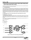
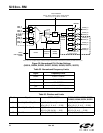
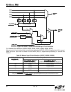
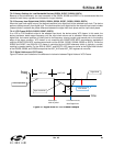
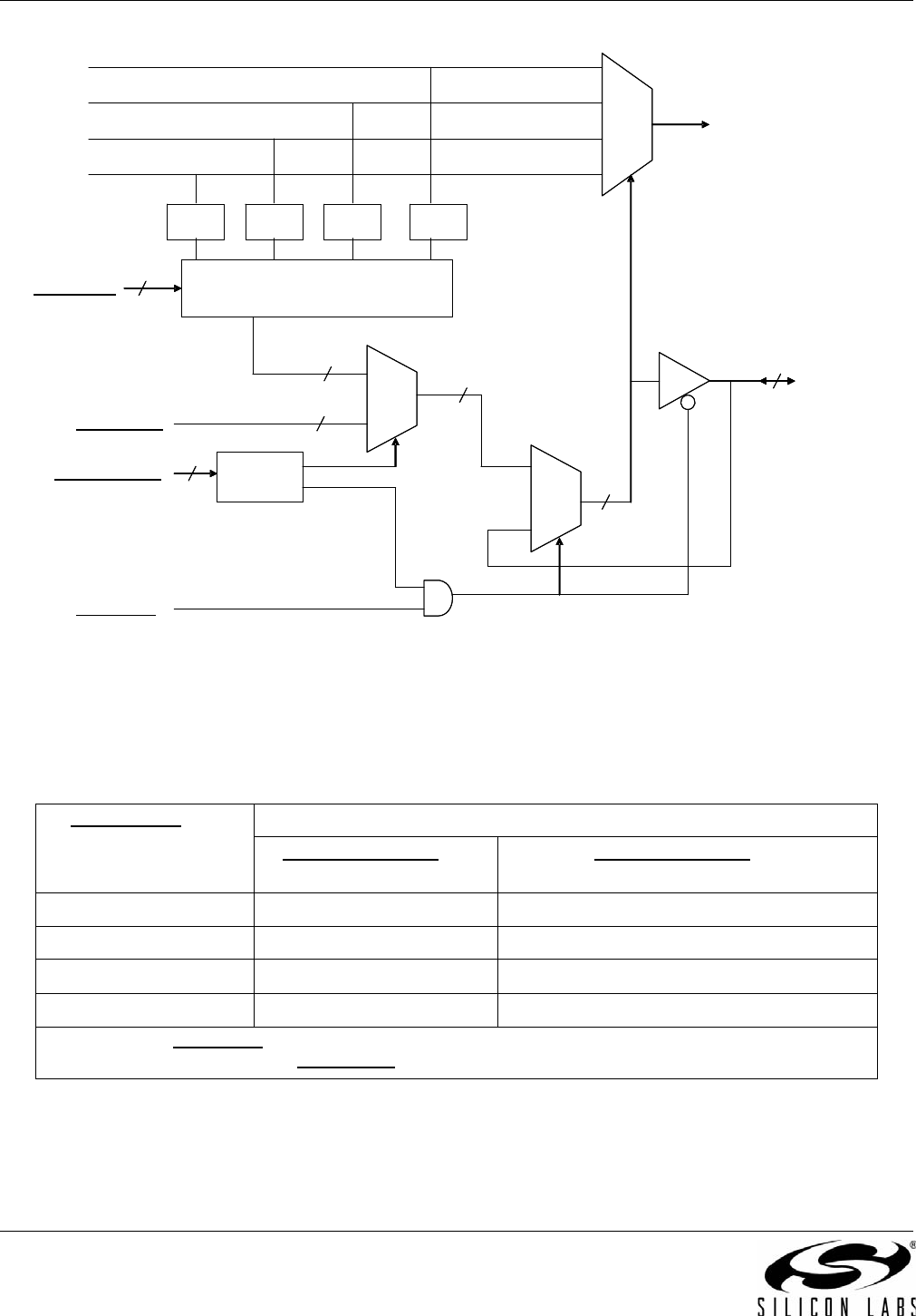
Figure 28. Si5367, Si5368, and Si5369 Input Clock Selection
7.4.1. Manual Clock Selection (Si5324, Si5325, Si5326, Si5367, Si5368, Si5369, Si5374)
Manual control of input clock selection is available by setting the AUTOSEL_REG[1:0] register bits to 00. In manual
mode, the active input clock is chosen via the CKSEL_REG[1:0] register setting according to Table 38 and
Table 39.
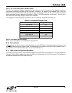
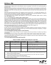
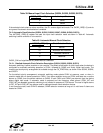
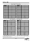
Table 38. Manual Input Clock Selection (Si5367, Si5368, Si5369)
CKSEL_REG[1:0]
Register Bits
Active Input Clock
CK_CONFIG_REG
= 0
(CKIN1,2,3,4 inputs)
CK_CONFIG_REG = 1
(CKIN1,3 & CKIN2,4 clock/FSYNC pairs)
00 CKIN1 CKIN1/CKIN3
01 CKIN2 CKIN2/CKIN4
10 CKIN3 Not used
11 CKIN4 Not used
Note: Setting the CKSEL_PIN register bit to one allows the CS [1:0] pins to continue to control input clock selection.
If CS_PIN is set to zero, the CKSEL_REG
[1:0] register bits perform the input clock selection function.
CKIN1
CKIN2
CKIN3
CKIN4
Clock priority logicCK_PRIORn
0
1
CKSEL_REG
AUTOSEL_REG 0
1
CKSEL_PIN
LOS/FOS
detect
LOS/FOS
detect
LOS/FOS
detect
LOS/FOS
detect
decode
Auto
Manual
Selected
Clock
2
2
2
2
2
8
2
CS0_C3A,
CS1_C4A
pins
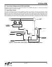
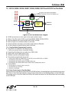
CKIN1
CKIN2
CKIN3
CKIN4
Clock priority logicCK_PRIORn
0
1
CKSEL_REG
AUTOSEL_REG 0
1
CKSEL_PIN
LOS/FOS
detect
LOS/FOS
detect
LOS/FOS
detect
LOS/FOS
detect
LOS/FOS
detect
LOS/FOS
detect
LOS/FOS
detect
LOS/FOS
detect
decode
Auto
Manual
Selected
Clock
2
2
2
2
2
8
2
CS0_C3A,
CS1_C4A
pins