


Si53xx-RM
Rev. 0.5 107
8.2. Output Clock Drivers
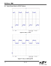
The output clocks can be configured to be compatible with LVPECL, CML, LVDS, or CMOS as shown in Table 56.
Unused outputs can be left unconnected. For microprocessor-controlled devices, it is recommended to write
“disable” to SFOUTn to disable the output buffer and reduce power. When the output mode is CMOS, bypass
mode is not supported.
8.2.1. LVPECL TQFP Output Signal Format Restrictions at 3.3 V (Si5367, Si5368, Si5369)
The LVPECL and CMOS output formats draw more current than either LVDS or CML; however, there are
restrictions in the allowed output format pin settings so that the maximum power dissipation for the TQFP devices
is limited when they are operated at 3.3 V. When Vdd = 3.3 V and there are four enabled LVPECL or CMOS
outputs, the fifth output must be disabled. When Vdd = 3.3 V and there are five enabled outputs, there can be no
more than three outputs that are either LVPECL or CMOS. All other configurations are valid, including those with
Vdd = 2.5 V.
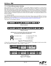
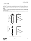
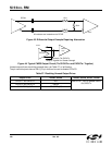
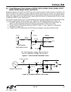
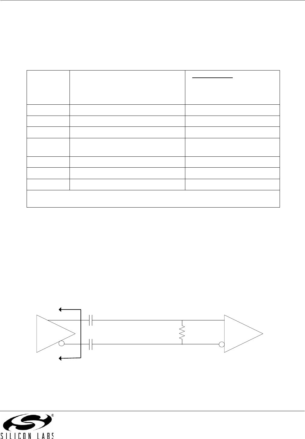
8.2.2. Typical Output Circuits
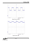
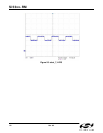
It is recommended that the outputs be ac coupled to avoid common mode issues. This suggestion does not apply
to the Si5366 and Si5368 when CKOUT5 is configured as FS_OUT (frame sync) because it can a have a duty
cycle significantly different from 50%.
Figure 42. Typical Output Circuit (Differential)
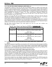
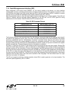
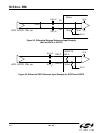
Table 56. Output Driver Configuration
Output Mode SFOUTn Pin Settings
(Si5316, Si5322, Si5323, Si5365)
SFOUTn_REG [2:0] Settings
(Si5319, Si5325, SI5326, Si5327,
Si5367, Si5368, Si5369, Si5374,
Si5375)
LVDS HM 111
CML HL 110
LVPECL MH 101
Low-swing
LVDS
ML 011
CMOS LH 010
Disabled LM 000
Reserved All Others All Others
Note: The LVPECL outputs are “LVPECL compatible.” No DC biasing circuitry is required to drive a
standard LVPECL load.
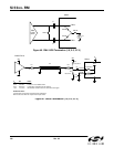
Si53xx
Rcvr
100
Z0 = 50
Z0 = 50