


Si53xx-RM
98 Rev. 0.5
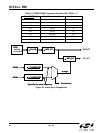
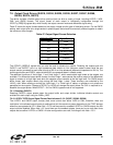
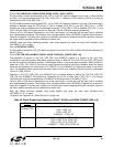
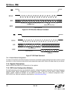
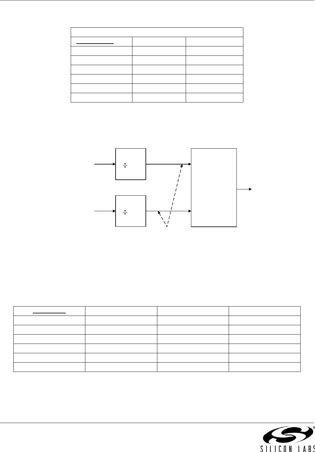
Both the FOS reference and the FOS monitored clock must be divided down to the same clock rate and this clock
rate must be between 10 MHz and 27 MHz. As can be seen in Figure 33, the values for P and Q must be selected
so that the FOS comparison occurs at the same frequency. The registers that contain the values for P and Q are
the CKINnRATE[2:0] registers.
Figure 33. FOS Compare
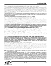
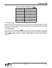
The frequency band of each input clock must be specified to use the FOS feature. The CLKNRATE registers
specify the frequency of the device input clocks as shown in Table 51.
When the FOS reference is the XA/XB oscillator (either internal or external), the value of Q in Figure 33 is always
2, for an effective CLKINnRATE of 1, as shown in Table 51.
For example, to monitor a 544 MHz clock at CKIN1 with a FOS reference of 34 MHz at CKIN2:
CLK1RATE = 5
CLK2RATE = 1
FOSREFSEL[2:0] = 010
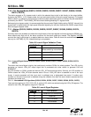
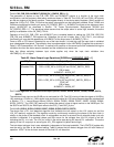
Table 50. FOS Reference Clock Selection
FOS Reference
FOSREFSEL
[2:0] Si5326 Si5368
000 XA/XB XA/XB
001 CKIN1 CKIN1
010 CKIN2 (default) CKIN2 (default)
011 Reserved CKIN3
100 Reserved CKIN4
all others Reserved Reserved
Table 51. CLKnRATE Registers
CLKnRATE Divisor, P or Q Min Frequency, MHz Max Frequency, MHz
0 1 10 27
1 2 25 54
2 4 50 105
3 8 95 215
416190435
532375710
CKIN
FOS_REF
P
Q
FOS
Compare
10 MHz min,
27 MHz max