


Si53xx-RM
32 Rev. 0.5
4. Device Specifications
The following tables are intended to simplify device selection. The specifications in the individual device data
sheets take precedence over this document. Refer to the respective device data sheet for devices not listed in the
tables below.
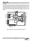
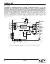
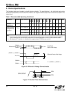
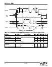
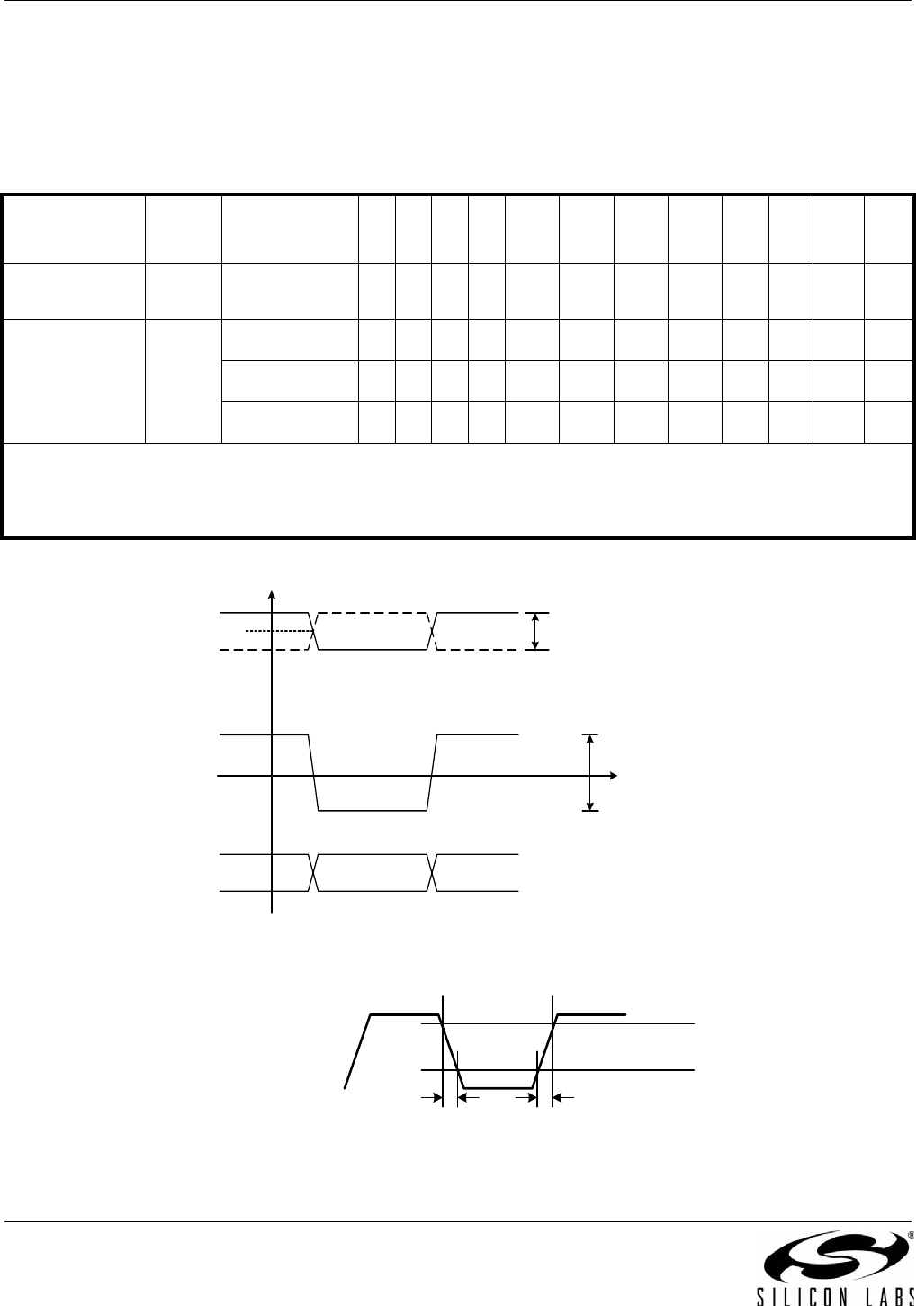
Figure 16. Differential Voltage Characteristics
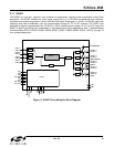
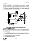
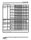
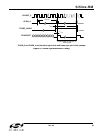
Figure 17. Rise/Fall Time Characteristics
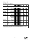
Table 3. Recommended Operating Conditions
1
Parameter Symbol Test Condition
Si5316
Si5322
Si5324
Si5325
Si5365
Si5366
Si5367
Si5368
Min Typ Max Unit
Ambient
Temperature
T
A
–40 25 85 ºC
Supply Voltage
During Normal
Operation
V
DD
3.3 V Nominal
Note 2 Note 2 Note 2 Note 2
2.97 3.3 3.63 V
2.5 V Nominal
2.25 2.5 2.75 V
1.8 V Nominal
1.71 1.8 1.89 V
Note:
1. All minimum and maximum specifications are guaranteed and apply across the recommended operating conditions.
Typical values apply at nominal supply voltages and an operating temperature of 25 ºC unless otherwise stated.
2. See Sections 6.7.1 and 8.2.1 for restrictions on output formats for TQFP devices at 3.3 V.
V
ISE
, V
OSE
V
ID
,V
OD
Differential I/Os
V
ICM
, V
OCM
Single-Ended
Peak-to-Peak Voltage
Differential Peak-to-Peak Voltage
SIGNAL +
SIGNAL –
(SIGNAL +) – (SIGNAL –)
V
t
SIGNAL +
SIGNAL –
V
ID
= (SIGNAL+) – (SIGNAL–)
V
ICM
, V
OCM
t
F
t
R
80%
20%
CKIN, CKOUT