Zeus
IOPS
3.5-Inch Fibre Channel Solid State Drive Product Manual Rev. 1.0 33
INTERFACE SPECIFICATIONS
SSD OPERATION
The Zeus
IOPS
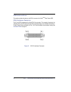
Fibre Channel SSD is comprised of the following primary functional blocks: the SCA-
2 interface connector, a Host FPGA, which contains a processor, NAND FPGA, NAND flash memory,
and DRAM.
Read/write data transfer requests are initiated by the host via the SCSI bus interface. Once received,
the Host FPGA controller, under the direction of the microcontroller, processes the request.
The FPGA NAND flash controller interfaces with the NAND flash chips and sequences the data flow
between the DRAM and flash.
Read and Write commands have dedicated hardware functions that do not require firmware support,
thereby increasing performance. Some commands may require the host controller to use external
circuitry that do not involve the flash memory controller.
When a Read or Write operation is requested, the integrated DMA controllers transfer the Fibre
Channel frames to and from the SSD DRAM.
It is the microcontroller that will initiate and monitor all
activity within the controller, including the execution of the
bad-block mapping and wear-leveling algorithms.
The controller will decode an incoming host command, and
will configure the appropriate interrupts and status for the
local microprocessor to handle various SCSI commands. For
read and write transfer commands, there are hardware
functions that minimize firmware overhead to enhance
performance.


