LZT 123 1836 31
5.3 General Electrical and Logical Characteristics
The electrical characteristics in this document refer to the behavior of the device
under specified conditions. Electrical requirements refer to conditions imposed on
the user for proper operation of the device.
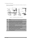
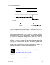
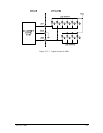
All IO to and from the GS64 is 1.8V unless otherwise stated. For user applications
employing other logic voltage technology it may be necessary to implement level
translators on the host-side circuitry in order to achieve level compatibility. To
facilitate ease of level conversion the GS64 provides a 1.8V reference on the VREF
pin. The VREF voltage from which all 1.8V logic is derived is covered in section 5.6
All input buffers are of the same type and they offer hysteresis of 200 mV—380 mV
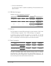
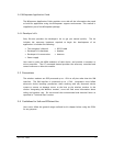
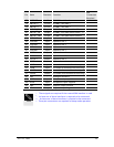
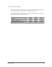
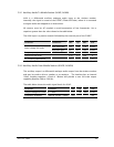
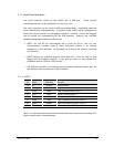
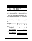
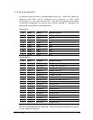
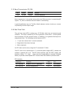
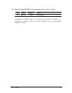
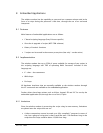
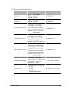
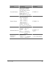
The electrical characteristics for 1.8V IO signals are shown in Table 5.3-1
Table 5.3-1 1.8V IO Characteristics
Parameter Min Typ Max Unit
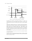
Input Voltage Low (VIL) –0.3 0.45 V
Input Voltage High (VIH) 1.16 VREF+0.3 V
Input Current (no pull-up) Low (VIL) 1.0
µA
Input Current (no pull-up) High (VIH) 1.0
µA
Output Low Voltage, 2 mA (VOL) 0.25 x VREF V
Output High Voltage, –2 mA (VOH) 0.75 x VREF V
Output 3-State Current Low (IOZL) 10
µA
Input Voltage Low (VIL) –0.3 0.45 V
Input Voltage Low (VIH) 1.16 VREF+0.3 V
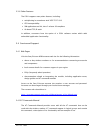
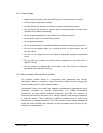
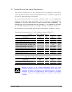
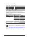
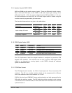
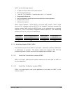
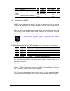
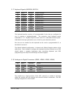
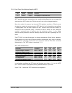
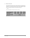
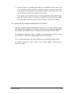
Table 5.3-2 1.8V IO Absolute Maximum Ratings
Parameter Min Typ Max Unit
Input Withstanding Voltage Low –0.5 V
Input Withstanding Voltage High 2.3 V
Stresses in excess of the voltage withstanding limits can cause
permanent damage to the device. These are absolute stress ratings only.
Functional operation of the device is not implied at these or any other
conditions in excess IO characteristics table. Exposure to absolute
maximum ratings for extended periods can adversely affect device
reliability.
!
WARNING