


Thales Computers 2-6 CPMC-1553R User’s Guide, CA.DT.356-0e
2.2.1.15 Expansion ROM Base Address Register The Expansion ROM Base Address Register is not
supported.
2.2.1.16 Interrupt Line Register The Interrupt Line Register is an 8-bit, read/write register that defines
which system interrupt request line (on the system interrupt controller) the INTA* output is routed. The
default value for this register is 0x00.
2.2.1.17 Interrupt Pin Register The Interrupt Pin Register is an 8-bit, read-only register that defines the
PCI interrupt generated by this board to be INTA*. This register returns a value of 0x01 when read.
2.2.1.18 Minimum Grant Register The minimum Grant Register is not supported.
2.2.1.19 Maximum Latency Register The Maximum Latency Register is not supported.
2.2.2 PCI Memory Space
The ACE registers, user defined discrete I/O, and ACE memory are all mapped to the PCI memory space.
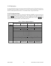
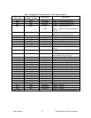
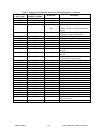
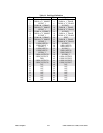
2.2.2.1 ACE Register Space The ACE register space is mapped into the PCI memory space. The
location of the ACE register and user defined discrete I/O is defined in Base Address Register 1 (BAR1),
address 0x14 in PCI configuration space. This space provides the software interface to the ACE device via
17 internal operational registers. The mapping of these registers is defined in Table 7. For more
information regarding the function of the register space of the ACE device, refer to the ILC-DDC data
sheet for BU-61688.