


Thales Computers 2-10 CPMC-1553R User’s Guide, CA.DT.356-0e
2.2.2.4 ACE Reset Register This read/write register is accessible at 0x0808, BAR 1. Only bit 0 is used.
After a PCI reset the register reads 0x00000001. To generate a reset to both ACE chips write a 0 to bit 0.
A 0 holds both ACEs in reset. Write a 1 to bit D0 to unreset both ACEs. This register is provided only for
test purposes and is not intended to be used as part of the normal CPMC-1553R operation.
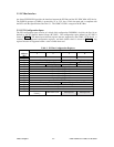
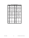
2.2.2.5 ACE Memory Space The ACE memory space is mapped into the PCI memory space. The
location of the ACE memory space is defined in BAR0, address 0x10 in PCI configuration space. All
registers are read/write and must be accessed as words only. The mapping of these registers is defined in
Table 10. For more information regarding the function of the memory space of the ACE device, refer to
the ILC-DDC data sheet for BU-61688.
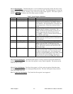
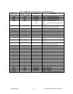
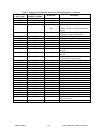
Table 10. ACE Memory Space Address Mapping
PCI Address
(AD19..AD0)
ACE Address
(ADDR15..ADDR0)
Description
00000 0000 ACE#1 – RAM location 0000
00002 0001 ACE#1 – RAM location 0001
00004 0002 ACE#1 – RAM location 0002
…… …
1FFFE FFFF ACE#1 – RAM location FFFF
20000 0000 ACE#2 – RAM location 0000
20002 0001 ACE#2 – RAM location 0001
20004 0002 ACE#2 – RAM location 0002
…… …
3FFFE FFFF ACE#2 – RAM location FFFF
40000 – 7FFFE Reserved