


2-12
X7DBU/X7DGU User's Manual
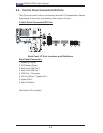
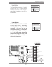
FP Power Butt
o
OH/Fan Fail/
PWR Fail/UID LED
1
NIC1 LED
FP Reset Butt
o
2
HDD LED
Power LED
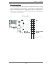
Reset
PWR
Vcc
UID Switch/Vcc
Vcc
Blue_LED_Cathode
(UID)/Vcc
Ground
Ground
1920
Vcc
X
Ground
NMI
X
Vcc
PWR Fail LED
NIC2 LED
Overheat (OH)/Fan Fail/PWR
Fail/FP UID LED
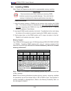
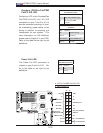
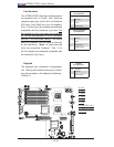
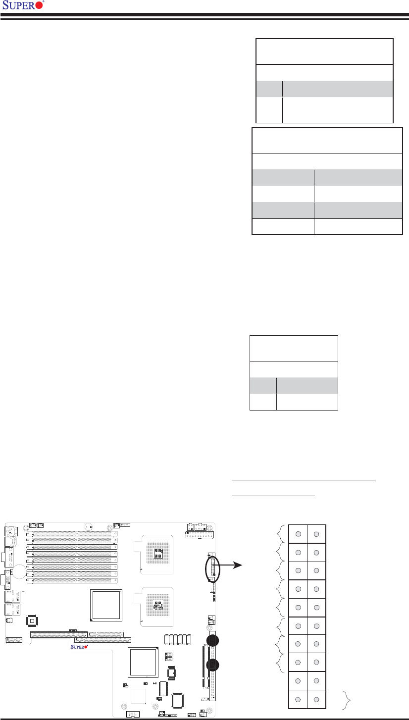
Connect an LED to the Overheat/Fan
Fail/PWR Fail/UID (Unit ID) LED
connection on pins 7 and 8 of JF1 to
provide advanced warnings of chas-
sis overheating, power failure or fan
failure in addition to providing unit
identifi cation for your system. (*For
more information on UID Switches,
please refer to Pages 2-11 and 2-22.)
Refer to the table on the right for pin
defi nitions.
Power Fail LED
The Power Fail LED connection is
located on pins 5 and 6 of JF1. Re-
fer to the table on the right for pin
defi nitions.
OH/Fan Fail/PWR Fail/FP UID LED
Pin Defi nitions (JF1)
Pin# Defi nition
7 Blue_LED_Cathode (UID)
8 OH_Fan Fail_PWR
Fail_UID
OH/Fan Fail/PWR Fail/FP UID Indica-
tor Status
State Defi nition
Off System Normal
Red On Overheat
Red Flashing Fan Fail/PWR Fail
Blue On FP UID
PWR Fail LED
Pin Defi nitions (JF1)
Pin# Defi nition
5 Vcc
6 Ground
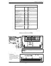
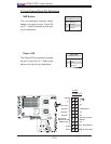
A
B
A. OH/Fan Fail/PWR Fail/UIE LED
B. PWR Supply Fail
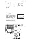
J
W
O
R
1
C
O
M2
J
7
J
B
T
1
J
W
O
L1
J
P
L1
J
P
L2
J
3
0
J
L1
J
O
H1
J
D
1
Fan2
LE
1
J
F1
FP
C
TRL
J
P
W
1
J
1
7
LE2
SW1
J11
I2
C
1
I2
C
2
J
P
G1
Rear UID
ES
1
0
0
0
Vide
o
C
T
R
L
In
t
e
l
E
S
B
2
(
S
o
u
th
B
ridg
e
)
U
S
B
4
J
W
D
J
K1
USB2
/
3
J
1
8
SMB
C
PU
1
J
P
W
3
COM1
VGA
LAN1
LAN2
J
2
8
SX
B
2
:
P
C
I-E
x
8
SXB1
:
P
C
I-E
x
1
6
P
C
I-X
1
3
3
M
Hz
(North Brid
g
e
)
V
ideo
Memo
ry
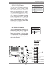
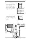
X7DBU
J
2
9
Fan4
Fan8
C
P
U
FA
N
2
Fan3
Fan1
2
0
-
P
in
Main
P
W
R
J
P
W
2
4
-P
in
P
W
R
8
-P
in
P
W
R
Fan7
C
P
U
Fan1
P
W
R
SM
B
Fan5
Fan6
B
uz
z
e
r
SP
1
J9B2
J9B1
J8B3
J8B2
J8B1
J7B3
J7B2
J7B1
D
IMM4
B
SGPIO
1
SGPIO
2
J
2
7
UIO
P
W
R
LA
N
C
T
R
L
J
LA
N
2
J
L
A
N
1
J
1
5
J
C
O
M1
J
KM1
Bank1
I-SA
T
A
0
I
-S
A
T
A
1
I-S
A
T
A
2
I
-S
A
T
A
3
I-SA
T
A
4
I-SA
T
A
5
B
IO
S
J
2
2
Floppy
SIMSO
ID
E#
1
C
PU
2
J
P
1
D
IMM1
A
D
IMM1
B
D
IMM2
A
D
I
M
M2
B
D
IMM3
A
D
IMM3
B
D
IMM4
A
Batte
ry
Bank2
Bank3
Bank4
KB/MS
USB 0/1
J
5
J14
S
I/
O
I
nte
l
5
0
0
0
J
9